- 您現(xiàn)在的位置:買賣IC網(wǎng) > PDF目錄43920 > LIT1108CS8-12#PBF (LINEAR TECHNOLOGY CORP) 1.5 A SWITCHING REGULATOR, 25 kHz SWITCHING FREQ-MAX, PDSO8 PDF資料下載
參數(shù)資料
| 型號: | LIT1108CS8-12#PBF |
| 廠商: | LINEAR TECHNOLOGY CORP |
| 元件分類: | 穩(wěn)壓器 |
| 英文描述: | 1.5 A SWITCHING REGULATOR, 25 kHz SWITCHING FREQ-MAX, PDSO8 |
| 封裝: | PLASTIC, SOIC-8 |
| 文件頁數(shù): | 3/12頁 |
| 文件大小: | 266K |
| 代理商: | LIT1108CS8-12#PBF |
11
LT1108
U
S
A
O
PPLICATI
WU
U
I FOR ATIO
Figure 8 details current limit circuitry. Sense transistor Q1,
whose base and emitter are paralleled with power switch
Q2, is ratioed such that approximately 0.5% of Q2’s
collector current flows in Q1’s collector. This current
passed through internal 80
resistor R1 and out through
the ILIM pin. The value of the external resistor connected
between ILIM and VIN sets the current limit. When sufficient
switch current flows to develop a VBE across R1 + RLIM, Q3
turns on and injects current into the oscillator, turning off
the switch. Delay through this circuitry is approximately
2
s. The current trip point becomes less accurate for
switch-ON times less than 5
s. Resistor values program-
ming switch-ON time for 2
s or less will cause spurious
response in the switch circuitry although the device will
still maintain output regulation.
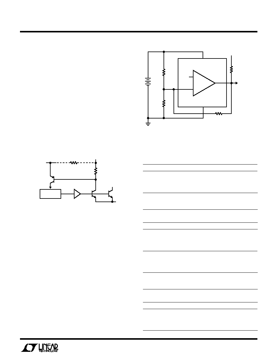
Figure 9. Setting Low Battery Detector Trip Point
LT1108 F09
R1
R2
1.245V
REF
SET
GND
IN
V
LT1108
47k
5V
TO
PROCESSOR
R1 =
VLB – 1.25V
35.1
A
VLB
+
–
AO
R3
= BATTERY TRIP POINT
R2 = 33k
R3 = 1.6M
VBAT
Table 1. Inductor Manufacturers
MANUFACTURER
PART NUMBERS
Coiltronics International
OCTA-PAC
TM
984 S.W. 13th Court
Series
Pompano Beach, FL 33069
305-781-8900
Sumida Electric Co. USA
CD54
708-956-0666
CDR74
CDR105
Table 2. Capacitor Manufacturers
MANUFACTURER
PART NUMBERS
Sanyo Video Components
OS-CON Series
1201 Sanyo Avenue
San Diego, CA 92073
619-661-6322
Nichicon America Corporation
PL Series
927 East State Parkway
Schaumberg, IL 60173
708-843-7500
AVX Corporation
TPS Series
Myrtle Beach, SC
803-946-0690
Table 3. Transistor Manufacturers
MANUFACTURER
PART NUMBERS
Zetex Inc.
ZTX 749 (NPN)
87 Modular Avenue
ZTX 849 (NPN)
Commack, NY 11725
ZTX 949 (PNP)
516-543-7100
Information furnished by Linear Technology Corporation is believed to be accurate and reliable.
However, no responsibility is assumed for its use. Linear Technology Corporation makes no represen-
tation that the interconnection of its circuits as described herein will not infringe on existing patent rights.
USING THE GAIN BLOCK
The gain block (GB) on the LT1108 can be used as an error
amplifier, low battery detector or linear post regulator. The
gain block itself is a very simple PNP input op amp with an
open collector NPN output. The negative input of the gain
block is tied internally to the 1.245V reference. The positive
input comes out on the SET pin.
Arrangement of the gain block as a low battery detector
is straightforward. Figure 9 shows hookup. R1 and R2
need only be low enough in value so that the bias current
of the SET input does not cause large errors. 33k for R2
is adequate. R3 can be added to introduce a small amount
of hysteresis. This will cause the gain block to “snap”
when the trip point is reached. Values in the 1M to 10M
range are optimal. The addition however, of R3 will
change the trip point.
Figure 8. LT1108 Current Limit Circuitry
LT1108 F08
SW2
SW1
DRIVER
OSCILLATOR
VIN
ILIM
R1
80
(INTERNAL)
RLIM
(EXTERNAL)
Q1
Q2
Q3
相關(guān)PDF資料 |
PDF描述 |
|---|---|
| LK1001-7EDDT | 1-OUTPUT 150 W AC-DC REG PWR SUPPLY MODULE |
| LK1001-7ERD6TB1 | 1-OUTPUT 150 W AC-DC REG PWR SUPPLY MODULE |
| LK1001-7ERD6T | 1-OUTPUT 150 W AC-DC REG PWR SUPPLY MODULE |
| LK1001-7PD0 | 1-OUTPUT 150 W AC-DC REG PWR SUPPLY MODULE |
| LK1001-7RD1T | 1-OUTPUT 150 W AC-DC REG PWR SUPPLY MODULE |
相關(guān)代理商/技術(shù)參數(shù) |
參數(shù)描述 |
|---|---|
| LIT-2013 | 制造商:JST Manufacturing 功能描述: |
| LI-TB01 | 功能描述:開發(fā)板和工具包 - ARM DM365 LEOPARDBOARD DEVELOPMENT BOARD RoHS:否 制造商:Arduino 產(chǎn)品:Development Boards 工具用于評估:ATSAM3X8EA-AU 核心:ARM Cortex M3 接口類型:DAC, ICSP, JTAG, UART, USB 工作電源電壓:3.3 V |
| LI-TB02 | 功能描述:開發(fā)板和工具包 - ARM DM368 LEOPARDBOARD DEVELOPMENT BOARD RoHS:否 制造商:Arduino 產(chǎn)品:Development Boards 工具用于評估:ATSAM3X8EA-AU 核心:ARM Cortex M3 接口類型:DAC, ICSP, JTAG, UART, USB 工作電源電壓:3.3 V |
| LIT-DSD-860972-4 | 制造商:PCA 功能描述:LIT-DSD-860972-4 |
| LITERATURE ED 5 | 制造商:SOLA/HEVI-DUTY 功能描述:_ |
發(fā)布緊急采購,3分鐘左右您將得到回復(fù)。