- 您現(xiàn)在的位置:買賣IC網(wǎng) > PDF目錄98000 > LIS3LV02DQ (STMICROELECTRONICS) SPECIALTY ANALOG CIRCUIT, PQCC28 PDF資料下載
參數(shù)資料
| 型號(hào): | LIS3LV02DQ |
| 廠商: | STMICROELECTRONICS |
| 元件分類: | 模擬信號(hào)調(diào)理 |
| 英文描述: | SPECIALTY ANALOG CIRCUIT, PQCC28 |
| 封裝: | 7 X 7 MM, 1.9 MM HEIGHT, PLASTIC, QFN-28 |
| 文件頁數(shù): | 20/42頁 |
| 文件大小: | 379K |
| 代理商: | LIS3LV02DQ |
第1頁第2頁第3頁第4頁第5頁第6頁第7頁第8頁第9頁第10頁第11頁第12頁第13頁第14頁第15頁第16頁第17頁第18頁第19頁當(dāng)前第20頁第21頁第22頁第23頁第24頁第25頁第26頁第27頁第28頁第29頁第30頁第31頁第32頁第33頁第34頁第35頁第36頁第37頁第38頁第39頁第40頁第41頁第42頁

LIS3LV02DQ
7 Register Description
CD00047926
27/42
ST bit is used to activate the self test function. When the bit is set to one, an output change will
occur to the device outputs (refer to table 2 and 3 for specification) thus allowing to check the
functionality of the whole measurement chain.
Zen bit enables the Z-axis measurement channel when set to 1. The default value is 1.
Yen bit enables the Y-axis measurement channel when set to 1. The default value is 1.
Xen bit enables the X-axis measurement channel when set to 1. The default value is 1.
7.9
CTRL_REG2 (21h)
FS bit is used to select Full Scale value. After the device power-up the default full scale value is
+/-2g. In order to obtain a +/-6g full scale it is necessary to set FS bit to ‘1’.
BDU bit is used to inhibit output registers update until both upper and lower register parts are
read. In default mode (BDU= ‘0’) the output register values are updated continuously. If for any
reason it is not sure to read faster than output data rate it is recommended to set BDU bit to ‘1’.
In this way the content of output registers is not updated until both MSB and LSB are read
avoiding to read values related to different sample time.
BLE bit is used to select Big Endian or Little Endian representation for output registers. In Big
Endian’s one MSB acceleration value is located at addresses 28h (X-axis), 2Ah (Y-axis) and
2Ch (Z-axis) while LSB acceleration value is located at addresses 29h (X-axis), 2Bh (Y-axis)
and 2Dh (Z-axis). In Little Endian representation (Default, BLE=‘0‘) the order is inverted (refer
to data register description for more details).
BOOT bit is used to refresh the content of internal registers stored in the flash memory block.
At the device power up the content of the flash memory block is transferred to the internal
registers related to trimming functions to permit a good behavior of the device itself. If for any
reason the content of trimming registers was changed it is sufficient to use this bit to restore
correct values. When BOOT bit is set to ‘1’ the content of internal flash is copied inside
corresponding internal registers and it is used to calibrate the device. These values are factory
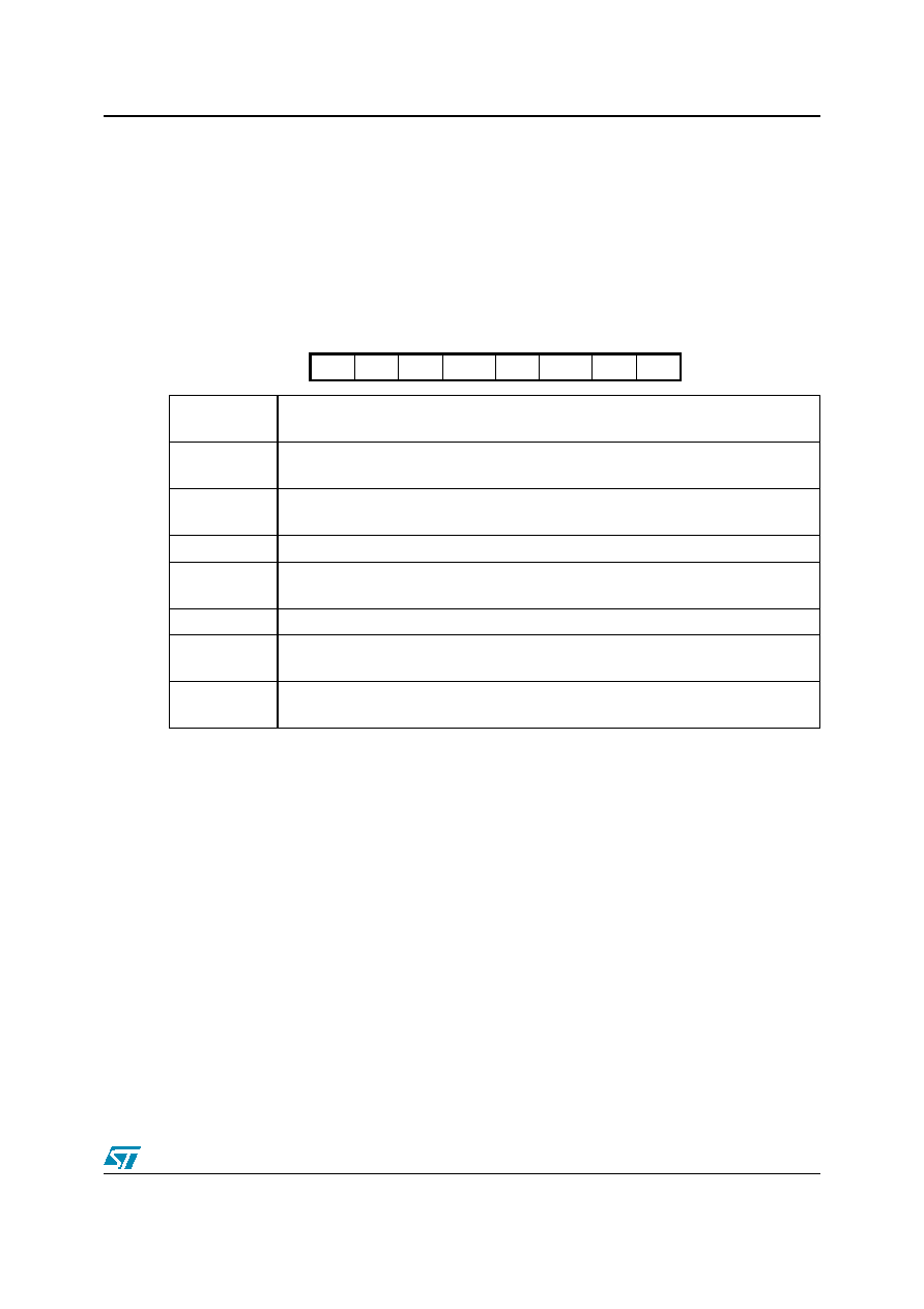
FS
BDU
BLE
BOOT
IEN
DRDY
SIM
DAS
FS
Full Scale selection
(0: ±2g; 1: ±6g)
BDU
Block Data Update
(0: continuous update; 1: output registers not updated until MSB and LSB reading)
BLE
Big/Little Endian selection
(0: little endian; 1: big endian)
BOOT
Reboot memory content
IEN
Interrupt ENable
(0: data ready on RDY pad; 1: int req on RDY pad)
DRDY
Enable Data-Ready generation
SIM
SPI Serial Interface Mode selection
(0: 4-wire interface; 1: 3-wire interface)
DAS
Data Alignment Selection
(0: 12 bit right justified; 1: 16 bit left justified)
相關(guān)PDF資料 |
PDF描述 |
|---|---|
| LKP5740-6R | 2-OUTPUT 250 W AC-DC PWR FACTOR CORR MODULE |
| LLT3837EFE | SWITCHING CONTROLLER, 110 kHz SWITCHING FREQ-MAX, PDSO16 |
| LM136AH-2.5/883B | 1-OUTPUT TWO TERM VOLTAGE REFERENCE, 2.5 V, MBCY3 |
| LM1946MX | 1-CHANNEL POWER SUPPLY SUPPORT CKT, PDSO20 |
| LM2316SLBX | PLL FREQUENCY SYNTHESIZER, 1200 MHz, CQCC16 |
相關(guān)代理商/技術(shù)參數(shù) |
參數(shù)描述 |
|---|---|
| LIS3LV02DQ-TR | 功能描述:加速計(jì) - 板上安裝 INERTIAL SENSOR Lo Vltg 3Axis RoHS:否 制造商:Murata 傳感軸:Double 加速:12 g 靈敏度: 封裝 / 箱體: 輸出類型:Analog 數(shù)字輸出 - 位數(shù):11 bit 電源電壓-最大:5.25 V 電源電壓-最小:4.75 V 電源電流:4 mA 最大工作溫度:+ 125 C 最小工作溫度:- 40 C |
| LIS3MDL | 制造商:STMicroelectronics 功能描述:DIGITAL OUTPUT MAGNETIC SENSOR ULTRA LOW-POWER, HIGH PERFORM - Trays |
| LIS3MDLTR | 制造商:STMicroelectronics 功能描述:ultra low-power, high performance 3-axis magnetometer |
| LIS-5-28 | 制造商:TDK-Lambda Corporation 功能描述:30.8W AC To DC Switching Power Supply - 95-132V/187-265V in - 28V 1.1A out |
| LIS-5-6 | 制造商:TDK-Lambda Corporation 功能描述:30W AC To DC Switching Power Supply - 95-132V/187-265V in - 6V 5A out |
發(fā)布緊急采購,3分鐘左右您將得到回復(fù)。