- 您現(xiàn)在的位置:買賣IC網(wǎng) > PDF目錄4588 > LFECP10E-3FN484C (Lattice Semiconductor Corporation)IC FPGA 10.2KLUTS 484FPBGA PDF資料下載
參數(shù)資料
| 型號(hào): | LFECP10E-3FN484C |
| 廠商: | Lattice Semiconductor Corporation |
| 文件頁數(shù): | 120/163頁 |
| 文件大小: | 0K |
| 描述: | IC FPGA 10.2KLUTS 484FPBGA |
| 標(biāo)準(zhǔn)包裝: | 60 |
| 系列: | ECP |
| 邏輯元件/單元數(shù): | 10200 |
| RAM 位總計(jì): | 282624 |
| 輸入/輸出數(shù): | 288 |
| 電源電壓: | 1.14 V ~ 1.26 V |
| 安裝類型: | 表面貼裝 |
| 工作溫度: | 0°C ~ 85°C |
| 封裝/外殼: | 484-BBGA |
| 供應(yīng)商設(shè)備封裝: | 484-FPBGA(23x23) |
第1頁第2頁第3頁第4頁第5頁第6頁第7頁第8頁第9頁第10頁第11頁第12頁第13頁第14頁第15頁第16頁第17頁第18頁第19頁第20頁第21頁第22頁第23頁第24頁第25頁第26頁第27頁第28頁第29頁第30頁第31頁第32頁第33頁第34頁第35頁第36頁第37頁第38頁第39頁第40頁第41頁第42頁第43頁第44頁第45頁第46頁第47頁第48頁第49頁第50頁第51頁第52頁第53頁第54頁第55頁第56頁第57頁第58頁第59頁第60頁第61頁第62頁第63頁第64頁第65頁第66頁第67頁第68頁第69頁第70頁第71頁第72頁第73頁第74頁第75頁第76頁第77頁第78頁第79頁第80頁第81頁第82頁第83頁第84頁第85頁第86頁第87頁第88頁第89頁第90頁第91頁第92頁第93頁第94頁第95頁第96頁第97頁第98頁第99頁第100頁第101頁第102頁第103頁第104頁第105頁第106頁第107頁第108頁第109頁第110頁第111頁第112頁第113頁第114頁第115頁第116頁第117頁第118頁第119頁當(dāng)前第120頁第121頁第122頁第123頁第124頁第125頁第126頁第127頁第128頁第129頁第130頁第131頁第132頁第133頁第134頁第135頁第136頁第137頁第138頁第139頁第140頁第141頁第142頁第143頁第144頁第145頁第146頁第147頁第148頁第149頁第150頁第151頁第152頁第153頁第154頁第155頁第156頁第157頁第158頁第159頁第160頁第161頁第162頁第163頁
2-3
Architecture
LatticeECP/EC Family Data Sheet
PFU and PFF Blocks
The core of the LatticeECP/EC devices consists of PFU and PFF blocks. The PFUs can be programmed to perform
Logic, Arithmetic, Distributed RAM and Distributed ROM functions. PFF blocks can be programmed to perform
Logic, Arithmetic and ROM functions. Except where necessary, the remainder of the data sheet will use the term
PFU to refer to both PFU and PFF blocks.
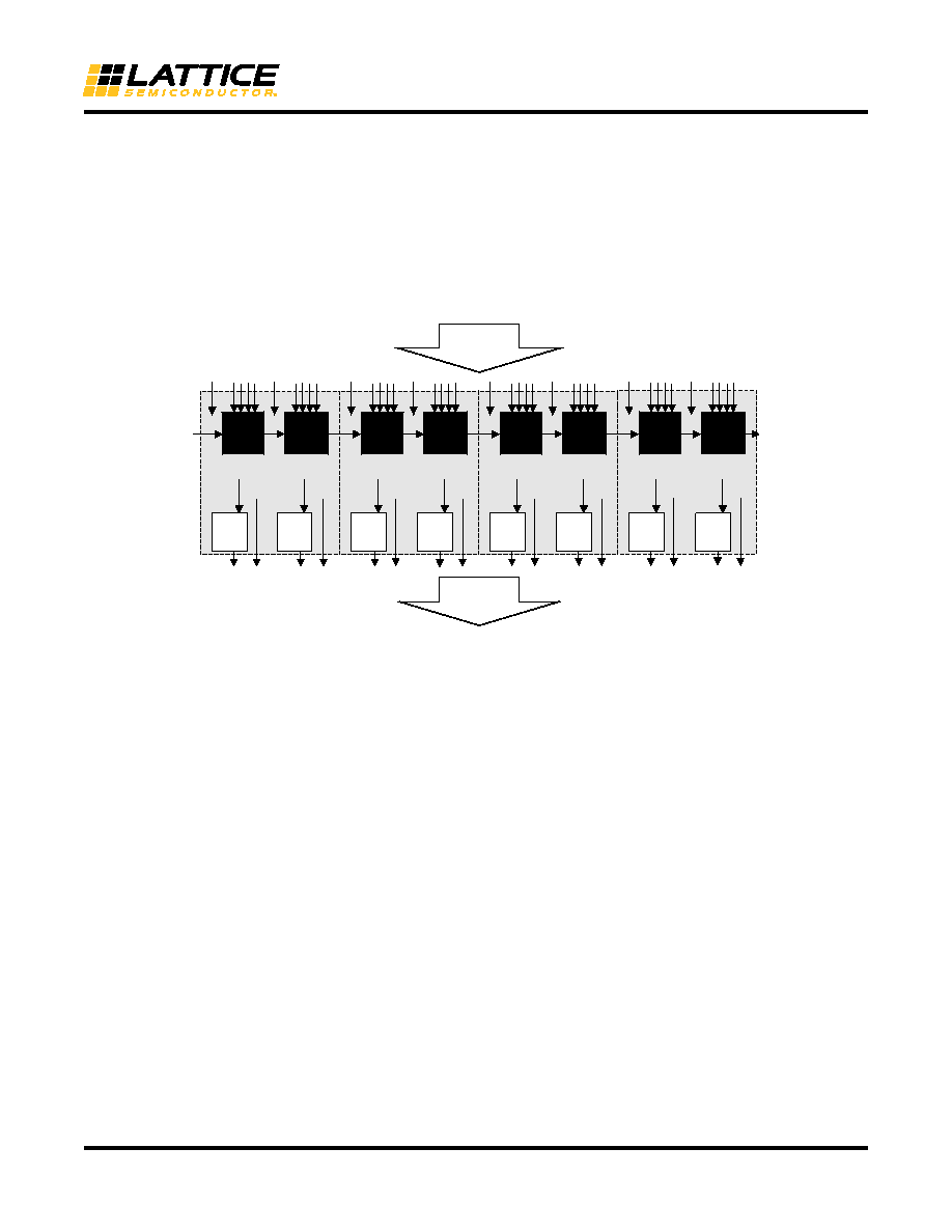
Each PFU block consists of four interconnected slices, numbered 0-3 as shown in Figure 2-3. All the interconnec-
tions to and from PFU blocks are from routing. There are 53 inputs and 25 outputs associated with each PFU block.
Figure 2-3. PFU Diagram
Slice
Each slice contains two LUT4 lookup tables feeding two registers (programmed to be in FF or Latch mode), and
some associated logic that allows the LUTs to be combined to perform functions such as LUT5, LUT6, LUT7 and
LUT8. There is control logic to perform set/reset functions (programmable as synchronous/asynchronous), clock
select, chip-select and wider RAM/ROM functions. Figure 2-4 shows an overview of the internal logic of the slice.
The registers in the slice can be configured for positive/negative and edge/level clocks.
There are 14 input signals: 13 signals from routing and one from the carry-chain (from adjacent slice or PFU).
There are 7 outputs: 6 to routing and one to carry-chain (to adjacent PFU). Table 2-1 lists the signals associated
with each slice.
Slice 0
LUT4 &
CARRY
LUT4 &
CARRY
FF/
Latch
D
FF/
Latch
D
Slice 1
LUT4 &
CARRY
LUT4 &
CARRY
Slice 2
LUT4 &
CARRY
LUT4 &
CARRY
From
Routing
To
Routing
Slice 3
LUT4 &
CARRY
LUT4 &
CARRY
FF/
Latch
D
FF/
Latch
D
FF/
Latch
D
FF/
Latch
D
FF/
Latch
D
FF/
Latch
D
相關(guān)PDF資料 |
PDF描述 |
|---|---|
| LFEC10E-3QN208C | IC FPGA 10.2KLUTS 147I/O 208QFP |
| IDT89HPES8NT2ZBBC | IC PCI SW 8LANE 2PORT 324-CABGA |
| IDT72V51236L7-5BB8 | IC FLOW CTRL MULTI QUEUE 256-BGA |
| IDT89HPES16NT2ZBBCG8 | IC PCI SW 16LANE 2PORT 484-CABGA |
| IDT89HPES16NT2ZBBC8 | IC PCI SW 16LANE 2PORT 484-CABGA |
相關(guān)代理商/技術(shù)參數(shù) |
參數(shù)描述 |
|---|---|
| LFECP10E-3FN484I | 功能描述:FPGA - 現(xiàn)場(chǎng)可編程門陣列 10.2K LUTs 288 I/O RoHS:否 制造商:Altera Corporation 系列:Cyclone V E 柵極數(shù)量: 邏輯塊數(shù)量:943 內(nèi)嵌式塊RAM - EBR:1956 kbit 輸入/輸出端數(shù)量:128 最大工作頻率:800 MHz 工作電源電壓:1.1 V 最大工作溫度:+ 70 C 安裝風(fēng)格:SMD/SMT 封裝 / 箱體:FBGA-256 |
| LFECP10E-3FN672C | 制造商:LATTICE 制造商全稱:Lattice Semiconductor 功能描述:LatticeECP/EC Family Data Sheet |
| LFECP10E-3FN672I | 制造商:LATTICE 制造商全稱:Lattice Semiconductor 功能描述:LatticeECP/EC Family Data Sheet |
| LFECP10E-3Q208C | 功能描述:FPGA - 現(xiàn)場(chǎng)可編程門陣列 10.2K LUTs RoHS:否 制造商:Altera Corporation 系列:Cyclone V E 柵極數(shù)量: 邏輯塊數(shù)量:943 內(nèi)嵌式塊RAM - EBR:1956 kbit 輸入/輸出端數(shù)量:128 最大工作頻率:800 MHz 工作電源電壓:1.1 V 最大工作溫度:+ 70 C 安裝風(fēng)格:SMD/SMT 封裝 / 箱體:FBGA-256 |
| LFECP10E-3Q208I | 功能描述:FPGA - 現(xiàn)場(chǎng)可編程門陣列 10.2K LUTs 147 I/O RoHS:否 制造商:Altera Corporation 系列:Cyclone V E 柵極數(shù)量: 邏輯塊數(shù)量:943 內(nèi)嵌式塊RAM - EBR:1956 kbit 輸入/輸出端數(shù)量:128 最大工作頻率:800 MHz 工作電源電壓:1.1 V 最大工作溫度:+ 70 C 安裝風(fēng)格:SMD/SMT 封裝 / 箱體:FBGA-256 |
發(fā)布緊急采購,3分鐘左右您將得到回復(fù)。