- 您現(xiàn)在的位置:買(mǎi)賣(mài)IC網(wǎng) > PDF目錄4587 > LFEC6E-4QN208I (Lattice Semiconductor Corporation)IC FPGA 6.1KLUTS 208PQFP PDF資料下載
參數(shù)資料
| 型號(hào): | LFEC6E-4QN208I |
| 廠商: | Lattice Semiconductor Corporation |
| 文件頁(yè)數(shù): | 84/163頁(yè) |
| 文件大?。?/td> | 0K |
| 描述: | IC FPGA 6.1KLUTS 208PQFP |
| 標(biāo)準(zhǔn)包裝: | 24 |
| 系列: | EC |
| 邏輯元件/單元數(shù): | 6100 |
| RAM 位總計(jì): | 94208 |
| 輸入/輸出數(shù): | 147 |
| 電源電壓: | 1.14 V ~ 1.26 V |
| 安裝類型: | 表面貼裝 |
| 工作溫度: | -40°C ~ 100°C |
| 封裝/外殼: | 208-BFQFP |
| 供應(yīng)商設(shè)備封裝: | 208-PQFP(28x28) |
第1頁(yè)第2頁(yè)第3頁(yè)第4頁(yè)第5頁(yè)第6頁(yè)第7頁(yè)第8頁(yè)第9頁(yè)第10頁(yè)第11頁(yè)第12頁(yè)第13頁(yè)第14頁(yè)第15頁(yè)第16頁(yè)第17頁(yè)第18頁(yè)第19頁(yè)第20頁(yè)第21頁(yè)第22頁(yè)第23頁(yè)第24頁(yè)第25頁(yè)第26頁(yè)第27頁(yè)第28頁(yè)第29頁(yè)第30頁(yè)第31頁(yè)第32頁(yè)第33頁(yè)第34頁(yè)第35頁(yè)第36頁(yè)第37頁(yè)第38頁(yè)第39頁(yè)第40頁(yè)第41頁(yè)第42頁(yè)第43頁(yè)第44頁(yè)第45頁(yè)第46頁(yè)第47頁(yè)第48頁(yè)第49頁(yè)第50頁(yè)第51頁(yè)第52頁(yè)第53頁(yè)第54頁(yè)第55頁(yè)第56頁(yè)第57頁(yè)第58頁(yè)第59頁(yè)第60頁(yè)第61頁(yè)第62頁(yè)第63頁(yè)第64頁(yè)第65頁(yè)第66頁(yè)第67頁(yè)第68頁(yè)第69頁(yè)第70頁(yè)第71頁(yè)第72頁(yè)第73頁(yè)第74頁(yè)第75頁(yè)第76頁(yè)第77頁(yè)第78頁(yè)第79頁(yè)第80頁(yè)第81頁(yè)第82頁(yè)第83頁(yè)當(dāng)前第84頁(yè)第85頁(yè)第86頁(yè)第87頁(yè)第88頁(yè)第89頁(yè)第90頁(yè)第91頁(yè)第92頁(yè)第93頁(yè)第94頁(yè)第95頁(yè)第96頁(yè)第97頁(yè)第98頁(yè)第99頁(yè)第100頁(yè)第101頁(yè)第102頁(yè)第103頁(yè)第104頁(yè)第105頁(yè)第106頁(yè)第107頁(yè)第108頁(yè)第109頁(yè)第110頁(yè)第111頁(yè)第112頁(yè)第113頁(yè)第114頁(yè)第115頁(yè)第116頁(yè)第117頁(yè)第118頁(yè)第119頁(yè)第120頁(yè)第121頁(yè)第122頁(yè)第123頁(yè)第124頁(yè)第125頁(yè)第126頁(yè)第127頁(yè)第128頁(yè)第129頁(yè)第130頁(yè)第131頁(yè)第132頁(yè)第133頁(yè)第134頁(yè)第135頁(yè)第136頁(yè)第137頁(yè)第138頁(yè)第139頁(yè)第140頁(yè)第141頁(yè)第142頁(yè)第143頁(yè)第144頁(yè)第145頁(yè)第146頁(yè)第147頁(yè)第148頁(yè)第149頁(yè)第150頁(yè)第151頁(yè)第152頁(yè)第153頁(yè)第154頁(yè)第155頁(yè)第156頁(yè)第157頁(yè)第158頁(yè)第159頁(yè)第160頁(yè)第161頁(yè)第162頁(yè)第163頁(yè)
2-24
Architecture
LatticeECP/EC Family Data Sheet
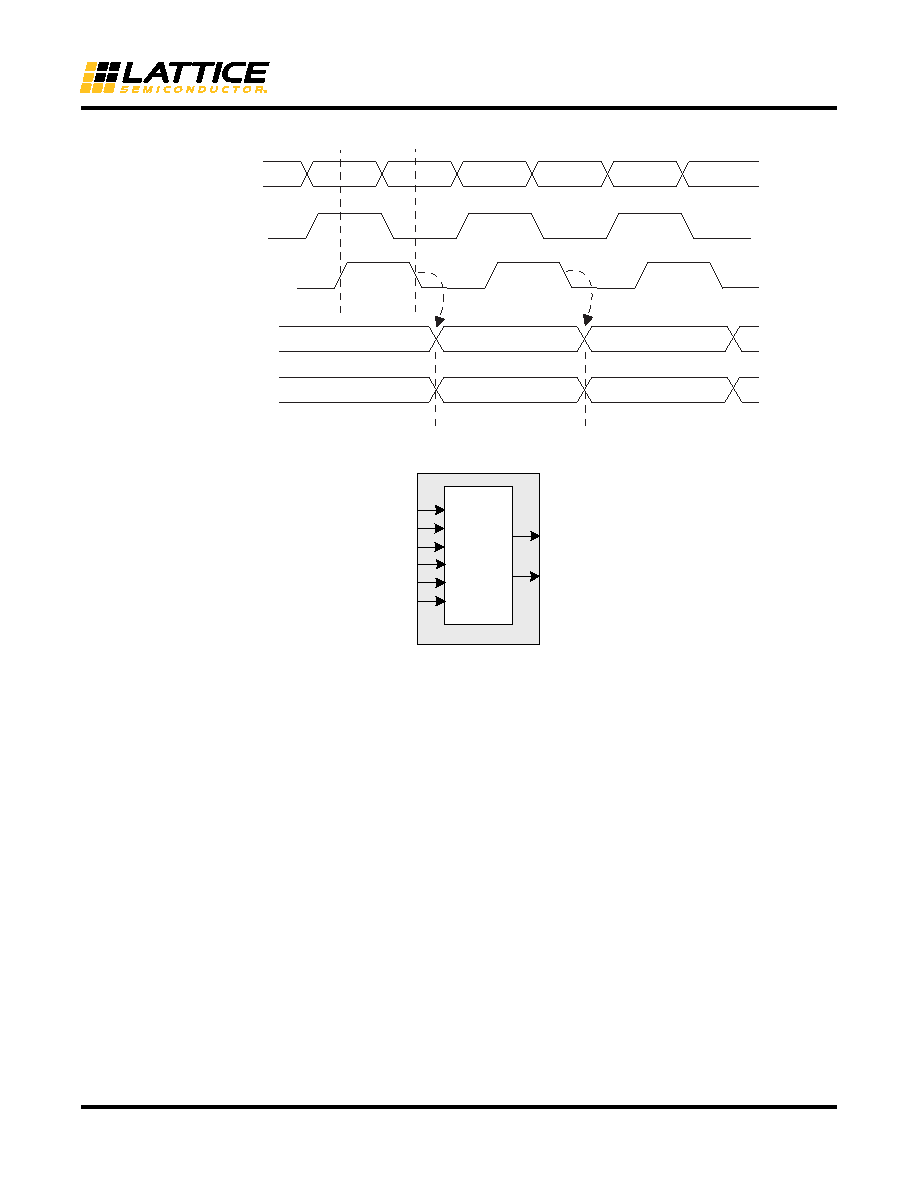
Figure 2-27. Input Register DDR Waveforms
Figure 2-28. INDDRXB Primitive
Output Register Block
The output register block provides the ability to register signals from the core of the device before they are passed
to the sysI/O buffers. The block contains a register for SDR operation that is combined with an additional latch for
DDR operation. Figure 2-29 shows the diagram of the Output Register Block.
In SDR mode, ONEG0 feeds one of the flip-flops that then feeds the output. The flip-flop can be configured a D-
type or latch. In DDR mode, ONEG0 is fed into one register on the positive edge of the clock and OPOS0 is
latched. A multiplexer running off the same clock selects the correct register for feeding to the output (D0).
Figure 2-30 shows the design tool DDR primitives. The SDR output register has reset and clock enable available.
The additional register for DDR operation does not have reset or clock enable available.
AB
C
D
E
F
BD
DI
(In DDR Mode)
D0
D2
DQS
A
C
DQS
Delayed
IDDRXB
LSR
QA
D
ECLK
QB
DDRCLKPOL
SCLK
CE
相關(guān)PDF資料 |
PDF描述 |
|---|---|
| LFEC6E-5QN208C | IC FPGA 6.1KLUTS 147I/O 208-PQFP |
| MIC5310-NKYML TR | IC REG LDO 2.85V/2.6V .15A 8-MLF |
| LT1963AMPS8#PBF | IC REG LDO ADJ 1.5A 8-SOIC |
| MIC5310-NDYML TR | IC REG LDO 2.85/1.85V .15A 8-MLF |
| RMA43DTAH | CONN EDGECARD 86POS R/A .125 SLD |
相關(guān)代理商/技術(shù)參數(shù) |
參數(shù)描述 |
|---|---|
| LFEC6E-4T100C | 制造商:LATTICE 制造商全稱:Lattice Semiconductor 功能描述:LatticeECP/EC Family Data Sheet |
| LFEC6E-4T100I | 制造商:LATTICE 制造商全稱:Lattice Semiconductor 功能描述:LatticeECP/EC Family Data Sheet |
| LFEC6E-4T144C | 功能描述:FPGA - 現(xiàn)場(chǎng)可編程門(mén)陣列 6.1 LUT 97 I/O RoHS:否 制造商:Altera Corporation 系列:Cyclone V E 柵極數(shù)量: 邏輯塊數(shù)量:943 內(nèi)嵌式塊RAM - EBR:1956 kbit 輸入/輸出端數(shù)量:128 最大工作頻率:800 MHz 工作電源電壓:1.1 V 最大工作溫度:+ 70 C 安裝風(fēng)格:SMD/SMT 封裝 / 箱體:FBGA-256 |
| LFEC6E-4T144I | 功能描述:FPGA - 現(xiàn)場(chǎng)可編程門(mén)陣列 6.1 LUT 97 I/O RoHS:否 制造商:Altera Corporation 系列:Cyclone V E 柵極數(shù)量: 邏輯塊數(shù)量:943 內(nèi)嵌式塊RAM - EBR:1956 kbit 輸入/輸出端數(shù)量:128 最大工作頻率:800 MHz 工作電源電壓:1.1 V 最大工作溫度:+ 70 C 安裝風(fēng)格:SMD/SMT 封裝 / 箱體:FBGA-256 |
| LFEC6E-4TN100C | 制造商:LATTICE 制造商全稱:Lattice Semiconductor 功能描述:LatticeECP/EC Family Data Sheet |
發(fā)布緊急采購(gòu),3分鐘左右您將得到回復(fù)。