- 您現(xiàn)在的位置:買賣IC網(wǎng) > PDF目錄4596 > LFEC3E-4TN100I (Lattice Semiconductor Corporation)IC FPGA 3.1KLUTS 100TQFP PDF資料下載
參數(shù)資料
| 型號: | LFEC3E-4TN100I |
| 廠商: | Lattice Semiconductor Corporation |
| 文件頁數(shù): | 85/163頁 |
| 文件大小: | 0K |
| 描述: | IC FPGA 3.1KLUTS 100TQFP |
| 標(biāo)準(zhǔn)包裝: | 90 |
| 系列: | EC |
| 邏輯元件/單元數(shù): | 3100 |
| RAM 位總計: | 56320 |
| 輸入/輸出數(shù): | 67 |
| 電源電壓: | 1.14 V ~ 1.26 V |
| 安裝類型: | 表面貼裝 |
| 工作溫度: | -40°C ~ 100°C |
| 封裝/外殼: | 100-LQFP |
| 供應(yīng)商設(shè)備封裝: | 100-TQFP(14x14) |
第1頁第2頁第3頁第4頁第5頁第6頁第7頁第8頁第9頁第10頁第11頁第12頁第13頁第14頁第15頁第16頁第17頁第18頁第19頁第20頁第21頁第22頁第23頁第24頁第25頁第26頁第27頁第28頁第29頁第30頁第31頁第32頁第33頁第34頁第35頁第36頁第37頁第38頁第39頁第40頁第41頁第42頁第43頁第44頁第45頁第46頁第47頁第48頁第49頁第50頁第51頁第52頁第53頁第54頁第55頁第56頁第57頁第58頁第59頁第60頁第61頁第62頁第63頁第64頁第65頁第66頁第67頁第68頁第69頁第70頁第71頁第72頁第73頁第74頁第75頁第76頁第77頁第78頁第79頁第80頁第81頁第82頁第83頁第84頁當(dāng)前第85頁第86頁第87頁第88頁第89頁第90頁第91頁第92頁第93頁第94頁第95頁第96頁第97頁第98頁第99頁第100頁第101頁第102頁第103頁第104頁第105頁第106頁第107頁第108頁第109頁第110頁第111頁第112頁第113頁第114頁第115頁第116頁第117頁第118頁第119頁第120頁第121頁第122頁第123頁第124頁第125頁第126頁第127頁第128頁第129頁第130頁第131頁第132頁第133頁第134頁第135頁第136頁第137頁第138頁第139頁第140頁第141頁第142頁第143頁第144頁第145頁第146頁第147頁第148頁第149頁第150頁第151頁第152頁第153頁第154頁第155頁第156頁第157頁第158頁第159頁第160頁第161頁第162頁第163頁
2-25
Architecture
LatticeECP/EC Family Data Sheet
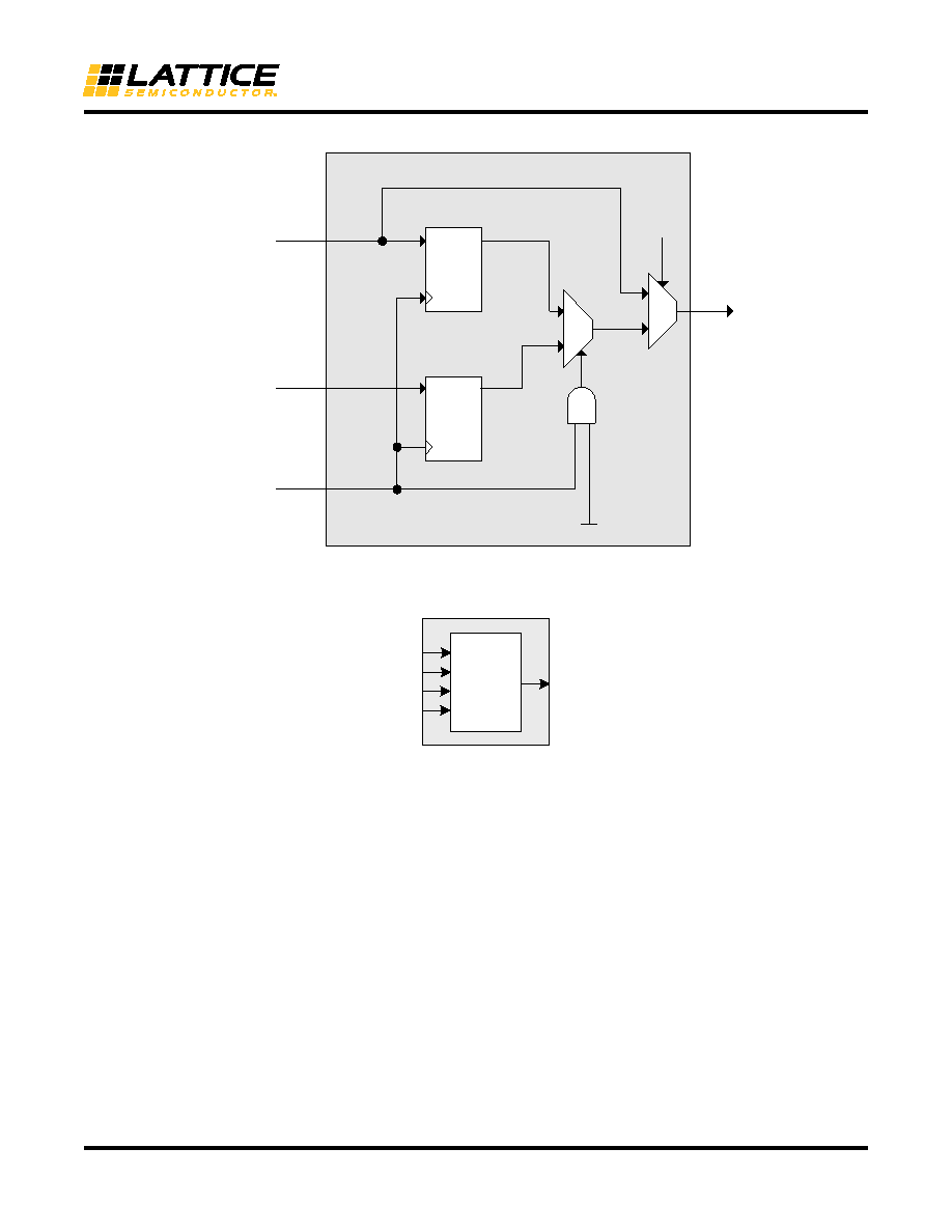
Figure 2-29. Output Register Block
Figure 2-30. ODDRXB Primitive
Tristate Register Block
The tristate register block provides the ability to register tri-state control signals from the core of the device before
they are passed to the sysI/O buffers. The block contains a register for SDR operation and an additional latch for
DDR operation. Figure 2-31 shows the diagram of the Tristate Register Block.
In SDR mode, ONEG1 feeds one of the flip-flops that then feeds the output. The flip-flop can be configured a D-
type or latch. In DDR mode, ONEG1 is fed into one register on the positive edge of the clock and OPOS1 is
latched. A multiplexer running off the same clock selects the correct register for feeding to the output (D0).
D
Q
D
Q
D-Type
ONEG0
From
Routing
CLK1
Programmed
Control
DO
Latch
LE*
*Latch is transparent when input is low.
OPOS0
OUTDDN
/LATCH
0
1
0
1
To sysIO
Buffer
ODDRXB
LSR
Q
DB
CLK
DA
相關(guān)PDF資料 |
PDF描述 |
|---|---|
| HSM43DSEF | CONN EDGECARD 86POS .156 EYELET |
| HMM43DSEF | CONN EDGECARD 86POS .156 EYELET |
| HSM43DRTF | CONN EDGECARD 86POS DIP .156 SLD |
| HMM43DRTF | CONN EDGECARD 86POS DIP .156 SLD |
| AMM22DRST | CONN EDGECARD 44POS DIP .156 SLD |
相關(guān)代理商/技術(shù)參數(shù) |
參數(shù)描述 |
|---|---|
| LFEC3E-4TN144C | 功能描述:FPGA - 現(xiàn)場可編程門陣列 3.1K LUTs Pb-Free RoHS:否 制造商:Altera Corporation 系列:Cyclone V E 柵極數(shù)量: 邏輯塊數(shù)量:943 內(nèi)嵌式塊RAM - EBR:1956 kbit 輸入/輸出端數(shù)量:128 最大工作頻率:800 MHz 工作電源電壓:1.1 V 最大工作溫度:+ 70 C 安裝風(fēng)格:SMD/SMT 封裝 / 箱體:FBGA-256 |
| LFEC3E-4TN144I | 功能描述:FPGA - 現(xiàn)場可編程門陣列 3.1K LUTs 97 IO 1.2V -4 Spd I RoHS:否 制造商:Altera Corporation 系列:Cyclone V E 柵極數(shù)量: 邏輯塊數(shù)量:943 內(nèi)嵌式塊RAM - EBR:1956 kbit 輸入/輸出端數(shù)量:128 最大工作頻率:800 MHz 工作電源電壓:1.1 V 最大工作溫度:+ 70 C 安裝風(fēng)格:SMD/SMT 封裝 / 箱體:FBGA-256 |
| LFEC3E-5F256C | 功能描述:FPGA - 現(xiàn)場可編程門陣列 3.1K LUTs RoHS:否 制造商:Altera Corporation 系列:Cyclone V E 柵極數(shù)量: 邏輯塊數(shù)量:943 內(nèi)嵌式塊RAM - EBR:1956 kbit 輸入/輸出端數(shù)量:128 最大工作頻率:800 MHz 工作電源電壓:1.1 V 最大工作溫度:+ 70 C 安裝風(fēng)格:SMD/SMT 封裝 / 箱體:FBGA-256 |
| LFEC3E-5F256CES | 功能描述:FPGA - 現(xiàn)場可編程門陣列 3.1 LUT 160 I/O RoHS:否 制造商:Altera Corporation 系列:Cyclone V E 柵極數(shù)量: 邏輯塊數(shù)量:943 內(nèi)嵌式塊RAM - EBR:1956 kbit 輸入/輸出端數(shù)量:128 最大工作頻率:800 MHz 工作電源電壓:1.1 V 最大工作溫度:+ 70 C 安裝風(fēng)格:SMD/SMT 封裝 / 箱體:FBGA-256 |
| LFEC3E-5F256I | 制造商:LATTICE 制造商全稱:Lattice Semiconductor 功能描述:LatticeECP/EC Family Data Sheet |
發(fā)布緊急采購,3分鐘左右您將得到回復(fù)。