- 您現(xiàn)在的位置:買賣IC網(wǎng) > PDF目錄367540 > LCD15C Direct ProTek Replacement:LCD15C PDF資料下載
參數(shù)資料
| 型號: | LCD15C |
| 英文描述: | Direct ProTek Replacement:LCD15C |
| 中文描述: | 直接太克替代:LCD15C |
| 文件頁數(shù): | 4/5頁 |
| 文件大?。?/td> | 147K |
| 代理商: | LCD15C |
4
www.protekdevices.com
LCD05C
thru
LCD24C
05018.R5 12/02
Circuit board Layout Recommendations
Circuit board layout is critical for Electromagnetic Compat-
ibility (EMC) protection. The following guidelines are
recommended:
The protection device should be placed near the input
terminals or connectors, the device will divert the
transient current immediately before it can be coupled
into the nearby traces.
The path length between the TVS devices and the
protected line should be minimized
All conductive loops including power and ground loops
should be minimized
The transient current return path to ground should be
kept as short as possible to reduce parasitic induc-
tance.
Ground planes should be used whenever possible.
For multilayer PCBs, use ground vias.
DEVICE SPECIFIC APPLICATION NOTE
The LCD Series are low capacitance, bidirectional TVS arrays that are designed to protect I/O or high speed data lines from the damaging effects of
ESD or EFT. This product series has a surge capability of 800 Watts P
PP
per line for an 8/20μs waveshape and offers ESD protection > 40kV.
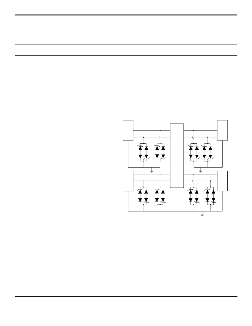
BIDIRECTIONAL COMMON MODE CONFIGURATION (Figure 1)
Ideal for use in USB applications, the LCD Series provides up to eight (8) lines of protection in a common mode configuration as depicted in Figure
1.
Circuit connectivity is as follows:
Pins 1, 2, 3, 4, 5, 6, 7, and 8 are connected to ground.
Pins 16 and 15 connected to Port #1 D- and D+.
Pins 14 and 13 connected to Port #2 D+ and D-.
Pins 12 and 11 connected to Port #3 D- and D+.
Pins 10 and 9 connected to Port #4 D+ and D-.
Figure 1. Typical Common- Mode USB Protection Circuit
D+
D-
U
C
D+
D-
D-
D+
USB OUTPUT
CONNECTOR
USB
IC
USB OUTPUT
CONNECTOR
U
C
D+
D-
3
4
2
1
5
8
7
6
16
15
14
13
12
11
10
9
PORT #1
PORT #2
PORT #4
PORT #3
相關(guān)PDF資料 |
PDF描述 |
|---|---|
| LCD24C | Direct ProTek Replacement:LCD24C |
| LCD1 | EM73201/EM73E00/EM73PE00 Application Note |
| LCD | |
| LCE2009S | NPN microwave power transistors |
| LCK4950 | Low-Voltage PLL Clock Driver |
相關(guān)代理商/技術(shù)參數(shù) |
參數(shù)描述 |
|---|---|
| LCD15C-LF | 制造商:ProTek Devices 功能描述:LOW CAPACITANCE TVS ARRAY 制造商:ProTek Devices 功能描述:LCD15C Series 6 Channel 38 Vcl 16.7 Vbr 15 pF Bidirectional TVS Array - DIP-16 |
| LCD160G032A | 制造商:VISHAY 制造商全稱:Vishay Siliconix 功能描述:160 x 32 Dots Graphic LCD |
| LCD-160G032A | 制造商:VISHAY 制造商全稱:Vishay Siliconix 功能描述:160 x 32 Dots Graphic LCD |
| LCD-160G032A_08 | 制造商:VISHAY 制造商全稱:Vishay Siliconix 功能描述:160 x 32 Dots Graphic LCD |
| LCD160G128B | 制造商:VISHAY 制造商全稱:Vishay Siliconix 功能描述:160 x 128 Dots Graphic LCD |
發(fā)布緊急采購,3分鐘左右您將得到回復(fù)。