- 您現(xiàn)在的位置:買(mǎi)賣(mài)IC網(wǎng) > PDF目錄30738 > LC99063-LF2 SPECIALTY CONSUMER CIRCUIT, PQFP100 PDF資料下載
參數(shù)資料
| 型號(hào): | LC99063-LF2 |
| 元件分類(lèi): | 消費(fèi)家電 |
| 英文描述: | SPECIALTY CONSUMER CIRCUIT, PQFP100 |
| 封裝: | SQFP-100 |
| 文件頁(yè)數(shù): | 2/8頁(yè) |
| 文件大小: | 149K |
| 代理商: | LC99063-LF2 |
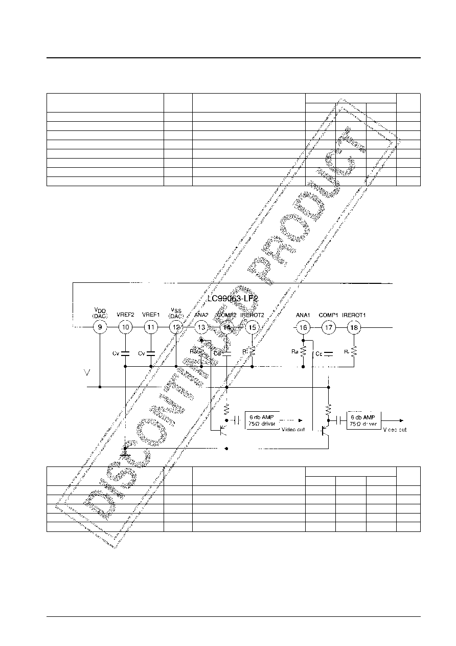
LC99063-LF2
Parameter
Symbol
Conditions
Ratings
Unit
min
typ
max
Input high-level voltage
VIH
CMOS level ; for pin type 1
0.7 VDD
V
Input low-level voltage
VIL
CMOS level ; for pin type 1
0.2 VDD
V
Input high-level voltage
VIH
CMOS level with Schmitt ; for pin type 2
0.75 VDD
V
Input low-level voltage
VIL
CMOS level with Schmitt ; for pin type 2
0.15 VDD
V
Output high-level voltage
VOH
IOH = –2 mA; for pin types 3 and 4
VDD – 0.8
V
Output low-level voltage
VOL
IOL = +2 mA; for pin types 3 and 4
0.4
V
Input leak current
IL
VI = VDD; for pin types 1 and 2
–10
+10
A
Output leak current
Ioz
High-impedance output; for pin type 3
–10
+10
A
Electrical Characteristics for Logic Circuits
DC Characteristics at Ta = –15 to +70°C, VDD = 3.0 to 3.6 V, VSS = 0 V
The pin types above refer to the following groups.
INPUT
(1) DIN [32:9], DEVICE, MIRRO, SUPER, INMODE, WBHL, DOSL, SSET [2:1], OMODE [4:1], RES
(2) DIN [8:1], CLK14M, CLK10M, HDI, VDI, HREF53, ENS, DATAS, CLKS, REGRES
OUTPUT
(3) DOUT [24:1]
(4) HREF, VDO, HDO, CLKOUT
Note: The ANA1, ANA2, IREFOT1, IREFOT2, VREF1, VREF2, COMP1, and COMP2 pins fall outside these DC characteristic specifications.
Electrical Characteristics for Analog Circuits
Recommended operating conditions for D/A converter
Parameter
Symbol
Conditions
Ratings
Unit
min
typ
max
Reference voltage
VREF1/2
1.11
V
Analog output resistance
Ra
200
Reference voltage resistance
Ri
Ra
× 4
Phase compensation capacitor
Cc
0.1
F
VREF capacitor
Cv
0.1
F
No. 5787-2/8
相關(guān)PDF資料 |
PDF描述 |
|---|---|
| LC99063 | SPECIALTY CONSUMER CIRCUIT |
| LC9907 | SPECIALTY CONSUMER CIRCUIT, PQFP64 |
| LCX017BL | SPECIALTY CONSUMER CIRCUIT |
| LCX023BM | SPECIALTY CONSUMER CIRCUIT |
| LCX026AL | SPECIALTY CONSUMER CIRCUIT |
相關(guān)代理商/技術(shù)參數(shù) |
參數(shù)描述 |
|---|---|
| LC99067MA0 | 制造商:未知廠家 制造商全稱(chēng):未知廠家 功能描述:Interface IC |
| LC99069ND3 | 制造商:未知廠家 制造商全稱(chēng):未知廠家 功能描述:Interface IC |
| LC9907 | 制造商:SANYO 制造商全稱(chēng):Sanyo Semicon Device 功能描述:Timing Generator for Solid-State Imager |
| LC99104 | 制造商:未知廠家 制造商全稱(chēng):未知廠家 功能描述:Area CCD Image Array |
| LC9911 | 制造商:未知廠家 制造商全稱(chēng):未知廠家 功能描述:Optoelectronic |
發(fā)布緊急采購(gòu),3分鐘左右您將得到回復(fù)。