- 您現(xiàn)在的位置:買賣IC網(wǎng) > PDF目錄358767 > LC7942YC (Sanyo Electric Co.,Ltd.) Dot Matrix LCD Driver(點(diǎn)陣LCD驅(qū)動器) PDF資料下載
參數(shù)資料
| 型號: | LC7942YC |
| 廠商: | Sanyo Electric Co.,Ltd. |
| 英文描述: | Dot Matrix LCD Driver(點(diǎn)陣LCD驅(qū)動器) |
| 中文描述: | 點(diǎn)陣LCD驅(qū)動器(點(diǎn)陣液晶驅(qū)動器) |
| 文件頁數(shù): | 5/8頁 |
| 文件大小: | 205K |
| 代理商: | LC7942YC |
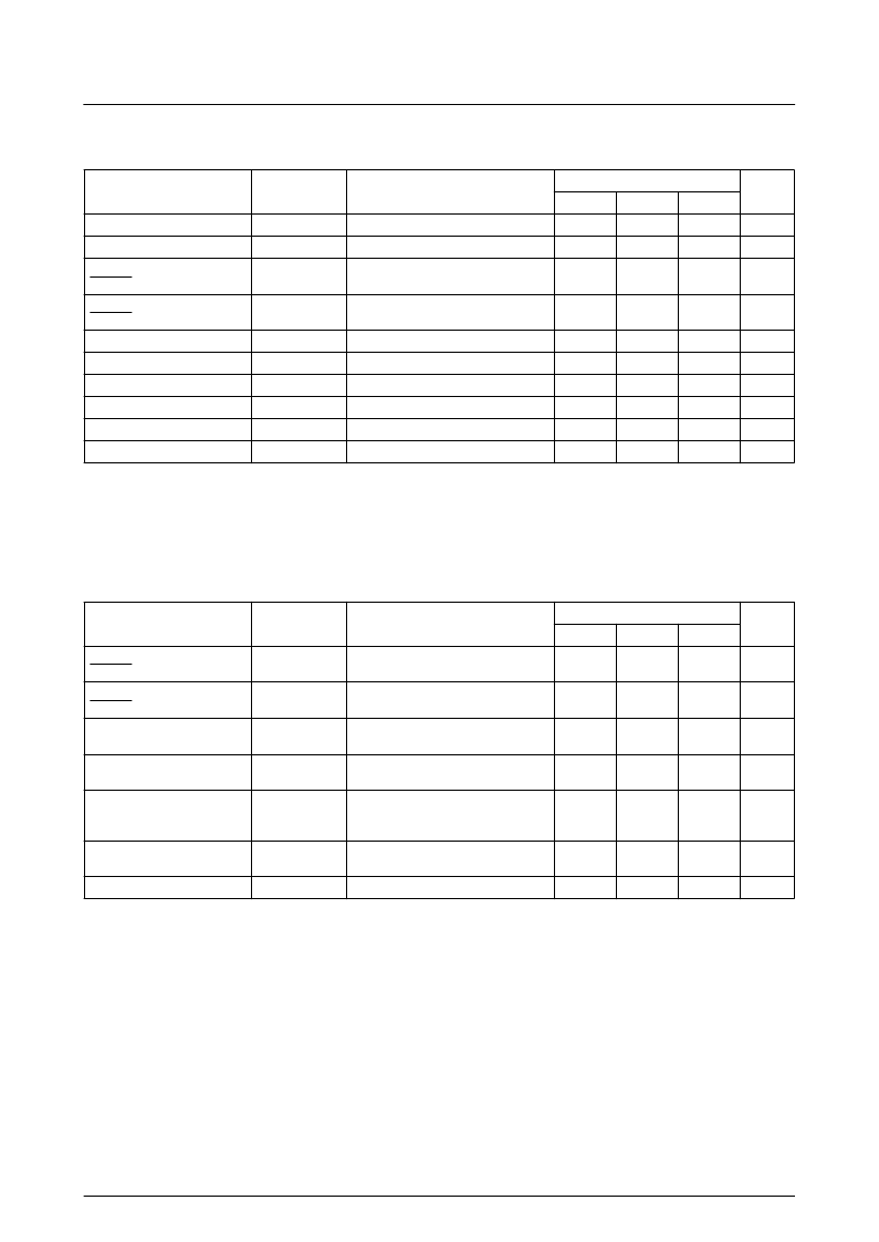
LC7942YC
No. 6159—5/8
Allowable Operating Ranges
at Ta = –20 to +85 °C, V
SS
= 0 V
Notes
1. V
2. At turn ON, the LCD supply should be energized after or simultaneously with the logic supply. At turn OFF, the logic supply
should be cut after or simultaneously with the LCD supply.
DD
≥
V
1
> V
2
> V
5
> V
EE
Electrical Characteristics
at Ta = 25 ± 2 C, V
SS
= 0 V, V
DD
= 2.7 to 5.5 V
Note
V
DE
= V
1
or V
2
or V
5
or V
EE
, V
l
= V
DD
, V
2
= 10/11
×
(V
DD
–
V
EE
), V
5
= l/11
×
(V
DD
–
V
EE
)
Parameter
Symbol
Conditions
Ratings
Unit
min
typ
–
–
max
Logic supply voltage
V
DD
2.7
5.5
V
LCD supply voltage
V
DD
– V
EE
See notes 1 and 2.
8
20
V
DIO1, DIO64, CP, M, RS/LS and
DISPOFF HIGH–level input voltage
V
IH
0.8V
DD
–
–
V
DIO1, DIO64, CP, M, RS/LS and
DISPOFF LOW–level input voltage
V
IL
–
–
0.2V
DD
V
CP shift clock frequency
f
CP
–
–
–
–
–
–
–
1
–
–
–
MHz
CP pulsewidth
t
WC
125
ns
DIO1 and DIO64 to CP setup time
t
SETUP
l00
ns
DIOI and DIOS4 to CP hold time
t
HOLD
l00
–
–
ns
CP rise time
t
R
50
ns
CP fall time
t
F
50
ns
Parameter
Symbol
Conditions
Ratings
Unit
min
typ
max
DIO1, DIO64, CP, M, RS/LS and
DISPOFF HIGH–level input current
I
IH
V
IN
= V
DD
–
–
1
μA
DIO1, DIO64, CP, M, RS/LS and
DISPOFF LOW–level input current
I
IL
V
IN
= V
SS
–
1
–
–
μA
DIO1 and DIO64 HIGH–level output
voltage
V
OH
I
OH
= –400 μA
V
DD
– 0.4
–
–
V
DIO1 and DIO64 LOW–level output
voltage
V
OL
I
OL
= 400 μA
–
–
0.4
V
O1 to O64 driver ON resistance
R
ON
V
DD
– V
EE
= 18 V,
V
DD
– V
OL
= 0.25 V,
V
DD
= 4.5 V
–
–
1.5
k
V
DD
static supply current
I
DD
V
DD
– V
EE
= 18 V,
CP = V
DD
–
–
100
μA
CP input capacitance
C
I
f
CP
= 1 MHz
–
5
–
pF
相關(guān)PDF資料 |
PDF描述 |
|---|---|
| LC7942YD | Dot Matrix LCD Driver(點(diǎn)陣LCD驅(qū)動器) |
| LC79430 | Dot Matrix LCD Driver |
| LC79430D | Dot Matrix LCD Driver |
| LC79431D | Dot Matrix LCD Driver |
| LC7943D | Dot Matrix LCD Driver |
相關(guān)代理商/技術(shù)參數(shù) |
參數(shù)描述 |
|---|---|
| LC7942YD | 制造商:未知廠家 制造商全稱:未知廠家 功能描述: |
| LC7943 | 制造商:未知廠家 制造商全稱:未知廠家 功能描述:Interface IC |
| LC79430 | 制造商:SANYO 制造商全稱:Sanyo Semicon Device 功能描述:Dot Matrix LCD Driver |
| LC79430D | 制造商:SANYO 制造商全稱:Sanyo Semicon Device 功能描述:Dot Matrix LCD Driver |
| LC79430KNE | 制造商:SANYO 制造商全稱:Sanyo Semicon Device 功能描述:Dot-Matrix LCD Drivers |
發(fā)布緊急采購,3分鐘左右您將得到回復(fù)。