- 您現(xiàn)在的位置:買賣IC網(wǎng) > PDF目錄19618 > LC5768VG-10F256I (Lattice Semiconductor Corporation)IC XPLD 768MC 10NS 256FPBGA PDF資料下載
參數(shù)資料
| 型號: | LC5768VG-10F256I |
| 廠商: | Lattice Semiconductor Corporation |
| 文件頁數(shù): | 4/99頁 |
| 文件大小: | 0K |
| 描述: | IC XPLD 768MC 10NS 256FPBGA |
| 標(biāo)準(zhǔn)包裝: | 90 |
| 系列: | ispMACH™ 5000VG |
| 可編程類型: | 系統(tǒng)內(nèi)可編程 |
| 最大延遲時間 tpd(1): | 10.0ns |
| 電壓電源 - 內(nèi)部: | 3 V ~ 3.6 V |
| 邏輯元件/邏輯塊數(shù)目: | 24 |
| 宏單元數(shù): | 768 |
| 輸入/輸出數(shù): | 196 |
| 工作溫度: | -40°C ~ 105°C |
| 安裝類型: | 表面貼裝 |
| 封裝/外殼: | 256-BGA |
| 供應(yīng)商設(shè)備封裝: | 256-FPBGA(17x17) |
| 包裝: | 托盤 |
第1頁第2頁第3頁當(dāng)前第4頁第5頁第6頁第7頁第8頁第9頁第10頁第11頁第12頁第13頁第14頁第15頁第16頁第17頁第18頁第19頁第20頁第21頁第22頁第23頁第24頁第25頁第26頁第27頁第28頁第29頁第30頁第31頁第32頁第33頁第34頁第35頁第36頁第37頁第38頁第39頁第40頁第41頁第42頁第43頁第44頁第45頁第46頁第47頁第48頁第49頁第50頁第51頁第52頁第53頁第54頁第55頁第56頁第57頁第58頁第59頁第60頁第61頁第62頁第63頁第64頁第65頁第66頁第67頁第68頁第69頁第70頁第71頁第72頁第73頁第74頁第75頁第76頁第77頁第78頁第79頁第80頁第81頁第82頁第83頁第84頁第85頁第86頁第87頁第88頁第89頁第90頁第91頁第92頁第93頁第94頁第95頁第96頁第97頁第98頁第99頁
Lattice Semiconductor
ispXPLD 5000MX Family Data Sheet
8
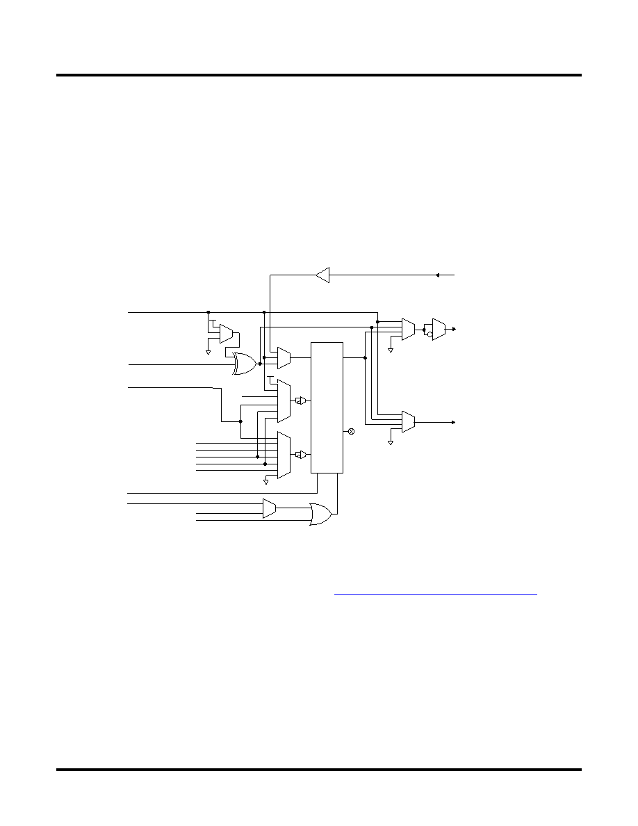
Macrocell
The 32 registered macrocells in the MFB are driven by the 32 outputs from the PTSA or the PTSA bypass. Each
macrocell contains a programmable XOR gate, a programmable register/latch flip-flop and the necessary clocks
and control logic to allow combinatorial or registered operation. All macrocells have an output that feeds the GRP.
Selected macrocells have an additional output that feeds the OSA and hence I/Os. This dual or concurrent output
capability from the macrocell gives efficient use of the hardware resources. One output can be a registered function
for example, while the other output can be an unrelated combinatorial function. A direct register input from the I/O
cell facilitates efficient use of the macrocell to construct high-speed input registers. Macrocell registers can be
clocked from one of several global or product term clocks available on the device. A global and product term clock
enable is also provided, eliminating the need to gate the clock to the macrocell registers directly. Reset and preset
for the macrocell register is provided from both global and product term signals. The macrocell register can be pro-
grammed to operate as a D-type register or a D-type latch. Figure 8 is a graphical representation of the macrocell.
Figure 8. Macrocell
Memory Modes
The ispXPLD 5000MX architecture allows the MFB to be configured as a variety of memory blocks as detailed in
Table 4. The remainder of this section details operation of each of the memory modes. Additional information
regarding the memory modes can also be found in TN1030, Using Memory in ispXPLD 5000MX Devices.
PTSA Bypass
From
I/O Cell
Output to
I/O Block
GRP
PT Clock
From PTSA
PT Preset
PT Reset
Shared PT Reset
Shared
PT CE
CLK0
CLK1
Shared PT Clock
CLK2
CLK3
Global Reset
Clk En
Clk
R/L
D
PR
Q
SELECT
DEVICES
DISCONTINUED
相關(guān)PDF資料 |
PDF描述 |
|---|---|
| EBM06DCBT-S189 | CONN EDGECARD 12POS R/A .156 SLD |
| RPER72A472K2P1A03B | CAP CER 4700PF 100V 10% RADIAL |
| GSM06DTAN-S189 | CONN EDGECARD 12POS R/A .156 SLD |
| RPER72A222K2P1A03B | CAP CER 2200PF 100V 10% RADIAL |
| TPME687K004R0018 | CAP TANT 680UF 4V 10% 2917 |
相關(guān)代理商/技術(shù)參數(shù) |
參數(shù)描述 |
|---|---|
| LC5768VG-10F484C | 功能描述:CPLD - 復(fù)雜可編程邏輯器件 PROGRAM EXPANDED LOG RoHS:否 制造商:Lattice 系列: 存儲類型:EEPROM 大電池?cái)?shù)量:128 最大工作頻率:333 MHz 延遲時間:2.7 ns 可編程輸入/輸出端數(shù)量:64 工作電源電壓:3.3 V 最大工作溫度:+ 90 C 最小工作溫度:0 C 封裝 / 箱體:TQFP-100 |
| LC5768VG-10F484I | 功能描述:CPLD - 復(fù)雜可編程邏輯器件 PROGRAM EXPANDED LOG RoHS:否 制造商:Lattice 系列: 存儲類型:EEPROM 大電池?cái)?shù)量:128 最大工作頻率:333 MHz 延遲時間:2.7 ns 可編程輸入/輸出端數(shù)量:64 工作電源電壓:3.3 V 最大工作溫度:+ 90 C 最小工作溫度:0 C 封裝 / 箱體:TQFP-100 |
| LC5768VG-12F256I | 功能描述:CPLD - 復(fù)雜可編程邏輯器件 PROGRAM EXPANDED LOG RoHS:否 制造商:Lattice 系列: 存儲類型:EEPROM 大電池?cái)?shù)量:128 最大工作頻率:333 MHz 延遲時間:2.7 ns 可編程輸入/輸出端數(shù)量:64 工作電源電壓:3.3 V 最大工作溫度:+ 90 C 最小工作溫度:0 C 封裝 / 箱體:TQFP-100 |
| LC5768VG-12F484I | 功能描述:CPLD - 復(fù)雜可編程邏輯器件 PROGRAM EXPANDED LOG RoHS:否 制造商:Lattice 系列: 存儲類型:EEPROM 大電池?cái)?shù)量:128 最大工作頻率:333 MHz 延遲時間:2.7 ns 可編程輸入/輸出端數(shù)量:64 工作電源電壓:3.3 V 最大工作溫度:+ 90 C 最小工作溫度:0 C 封裝 / 箱體:TQFP-100 |
| LC5768VG-5F256C | 功能描述:CPLD - 復(fù)雜可編程邏輯器件 PROGRAM EXPANDED LOG RoHS:否 制造商:Lattice 系列: 存儲類型:EEPROM 大電池?cái)?shù)量:128 最大工作頻率:333 MHz 延遲時間:2.7 ns 可編程輸入/輸出端數(shù)量:64 工作電源電壓:3.3 V 最大工作溫度:+ 90 C 最小工作溫度:0 C 封裝 / 箱體:TQFP-100 |
發(fā)布緊急采購,3分鐘左右您將得到回復(fù)。