- 您現(xiàn)在的位置:買(mǎi)賣(mài)IC網(wǎng) > PDF目錄19627 > LC51024MV-75F672I (Lattice Semiconductor Corporation)IC XPLD 1024MC 7.5NS 672FPBGA PDF資料下載
參數(shù)資料
| 型號(hào): | LC51024MV-75F672I |
| 廠商: | Lattice Semiconductor Corporation |
| 文件頁(yè)數(shù): | 8/99頁(yè) |
| 文件大小: | 0K |
| 描述: | IC XPLD 1024MC 7.5NS 672FPBGA |
| 標(biāo)準(zhǔn)包裝: | 40 |
| 系列: | ispXPLD® 5000MV |
| 可編程類(lèi)型: | 系統(tǒng)內(nèi)可編程 |
| 最大延遲時(shí)間 tpd(1): | 7.5ns |
| 電壓電源 - 內(nèi)部: | 3 V ~ 3.6 V |
| 邏輯元件/邏輯塊數(shù)目: | 32 |
| 宏單元數(shù): | 1024 |
| 輸入/輸出數(shù): | 381 |
| 工作溫度: | -40°C ~ 105°C |
| 安裝類(lèi)型: | 表面貼裝 |
| 封裝/外殼: | 672-BBGA |
| 供應(yīng)商設(shè)備封裝: | 672-FPBGA(27x27) |
| 包裝: | 托盤(pán) |
第1頁(yè)第2頁(yè)第3頁(yè)第4頁(yè)第5頁(yè)第6頁(yè)第7頁(yè)當(dāng)前第8頁(yè)第9頁(yè)第10頁(yè)第11頁(yè)第12頁(yè)第13頁(yè)第14頁(yè)第15頁(yè)第16頁(yè)第17頁(yè)第18頁(yè)第19頁(yè)第20頁(yè)第21頁(yè)第22頁(yè)第23頁(yè)第24頁(yè)第25頁(yè)第26頁(yè)第27頁(yè)第28頁(yè)第29頁(yè)第30頁(yè)第31頁(yè)第32頁(yè)第33頁(yè)第34頁(yè)第35頁(yè)第36頁(yè)第37頁(yè)第38頁(yè)第39頁(yè)第40頁(yè)第41頁(yè)第42頁(yè)第43頁(yè)第44頁(yè)第45頁(yè)第46頁(yè)第47頁(yè)第48頁(yè)第49頁(yè)第50頁(yè)第51頁(yè)第52頁(yè)第53頁(yè)第54頁(yè)第55頁(yè)第56頁(yè)第57頁(yè)第58頁(yè)第59頁(yè)第60頁(yè)第61頁(yè)第62頁(yè)第63頁(yè)第64頁(yè)第65頁(yè)第66頁(yè)第67頁(yè)第68頁(yè)第69頁(yè)第70頁(yè)第71頁(yè)第72頁(yè)第73頁(yè)第74頁(yè)第75頁(yè)第76頁(yè)第77頁(yè)第78頁(yè)第79頁(yè)第80頁(yè)第81頁(yè)第82頁(yè)第83頁(yè)第84頁(yè)第85頁(yè)第86頁(yè)第87頁(yè)第88頁(yè)第89頁(yè)第90頁(yè)第91頁(yè)第92頁(yè)第93頁(yè)第94頁(yè)第95頁(yè)第96頁(yè)第97頁(yè)第98頁(yè)第99頁(yè)
Lattice Semiconductor
ispXPLD 5000MX Family Data Sheet
12
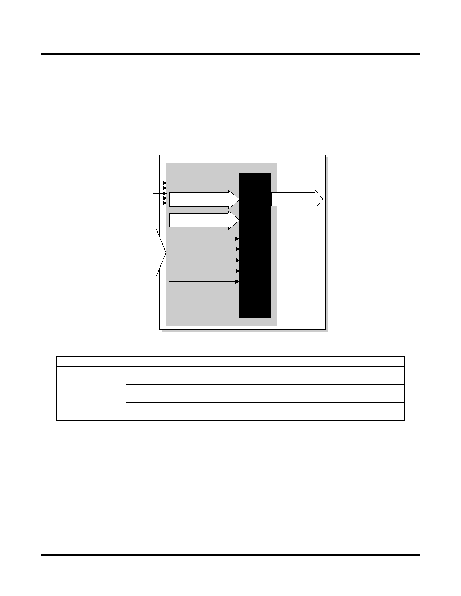
Single-Port SRAM Mode
In Single-Port SRAM Mode the multi-function array is configured as a single-port SRAM. In this mode one ports
accesses 16,384-bits of memory. Data widths of 1, 2, 4, 8, 16 and 32 are supported by the MFB. Figure 11 shows
the block diagram of the single-port SRAM.
Write data, address, chip select and read/write signals are always synchronous (registered.) The output data sig-
nals can be synchronous or asynchronous. Reset is asynchronous. All signals share a common clock, clock
enable, and reset. Table 7 shows the possible sources for the clock, clock enable and reset signals.
Figure 11. Single-Port SRAM Block Diagram
Table 7. Register Clock, Clock Enable, and Reset in Single-Port SRAM Mode
Register
Input
Source
Address, Write Data,
Read Data, Read/
Write, and Chip
Select
Clock
CLK or one of the global clocks (CLK0 - CLK3). Each of these signals can
be inverted if required.
Clock Enable
CEN or one of the global clocks (CLK1 - CLK 2). Each of these signals can
be inverted if required.
Reset
Created by the logical OR of the global reset signal and RST. RST is routed
by the multifunction array from GRP, with inversion if desired.
‘
68 Inputs
from
Routing
RESET
CLK0
CLK3
CLK1
CLK2
16,384-Bit
SRAM
Array
Clock (CLK)
Read/Write Address
(AD[0-8:13])
Write/Read (WR)
Chip Select (CS0,1)
Reset (RST)
Clk Enable (CEN)
Write Data
(DI[0-0,1,3,7,15,31])
Read Data
(DO[0-0,31])
SELECT
DEVICES
DISCONTINUED
相關(guān)PDF資料 |
PDF描述 |
|---|---|
| ATF750LVC-15SC | IC CPLD 15NS 24SOIC |
| FSEZ1317MY | IC PWM CTLR PRIMARY REG 7SOIC |
| GBM10DCCT | CONN EDGECARD 20POS R/A .156 SLD |
| VE-BTX-CY-F2 | CONVERTER MOD DC/DC 5.2V 50W |
| S271K25X5FN6UJ6R | CAP CER 270PF 1KV 10% RADIAL |
相關(guān)代理商/技術(shù)參數(shù) |
參數(shù)描述 |
|---|---|
| LC51024MV-75FN208C | 制造商:LATTICE 制造商全稱(chēng):Lattice Semiconductor 功能描述:3.3V, 2.5V and 1.8V In-System Programmable eXpanded Programmable Logic Device XPLD⑩ Family |
| LC51024MV-75FN208I | 制造商:LATTICE 制造商全稱(chēng):Lattice Semiconductor 功能描述:3.3V, 2.5V and 1.8V In-System Programmable eXpanded Programmable Logic Device XPLD⑩ Family |
| LC51024MV-75FN256C | 制造商:LATTICE 制造商全稱(chēng):Lattice Semiconductor 功能描述:3.3V, 2.5V and 1.8V In-System Programmable eXpanded Programmable Logic Device XPLD⑩ Family |
| LC51024MV-75FN256I | 制造商:LATTICE 制造商全稱(chēng):Lattice Semiconductor 功能描述:3.3V, 2.5V and 1.8V In-System Programmable eXpanded Programmable Logic Device XPLD⑩ Family |
| LC51024MV-75FN484C | 功能描述:CPLD - 復(fù)雜可編程邏輯器件 PROGRAM EXPANDED LOG RoHS:否 制造商:Lattice 系列: 存儲(chǔ)類(lèi)型:EEPROM 大電池?cái)?shù)量:128 最大工作頻率:333 MHz 延遲時(shí)間:2.7 ns 可編程輸入/輸出端數(shù)量:64 工作電源電壓:3.3 V 最大工作溫度:+ 90 C 最小工作溫度:0 C 封裝 / 箱體:TQFP-100 |
發(fā)布緊急采購(gòu),3分鐘左右您將得到回復(fù)。