- 您現(xiàn)在的位置:買賣IC網(wǎng) > PDF目錄30727 > LA7953 2 CHANNEL(S), TONE CONTROL CIRCUIT, PDIP30 PDF資料下載
參數(shù)資料
| 型號(hào): | LA7953 |
| 元件分類: | 音頻控制 |
| 英文描述: | 2 CHANNEL(S), TONE CONTROL CIRCUIT, PDIP30 |
| 封裝: | PLASTIC, SDIP-30 |
| 文件頁(yè)數(shù): | 1/7頁(yè) |
| 文件大小: | 146K |
| 代理商: | LA7953 |
Any and all SANYO products described or contained herein do not have specifications that can handle
applications that require extremely high levels of reliability, such as life-support systems, aircraft’s
control systems, or other applications whose failure can be reasonably expected to result in serious
physical and/or material damage. Consult with your SANYO representative nearest you before using
any SANYO products described or contained herein in such applications.
SANYO assumes no responsibility for equipment failures that result from using products at values that
exceed, even momentarily, rated values (such as maximum ratings, operating condition ranges,or other
parameters) listed in products specifications of any and all SANYO products described or contained
herein.
Monolithic Linear IC
Audio Controller for TV Use
Ordering number:ENN2713A
LA7953
SANYO Electric Co.,Ltd. Semiconductor Company
TOKYO OFFICE Tokyo Bldg., 1-10, 1 Chome, Ueno, Taito-ku, TOKYO, 110-8534 JAPAN
12501TN (KT)/O2095TH (KOTO)/7128TA, TS (KOTO) No.2713–1/7
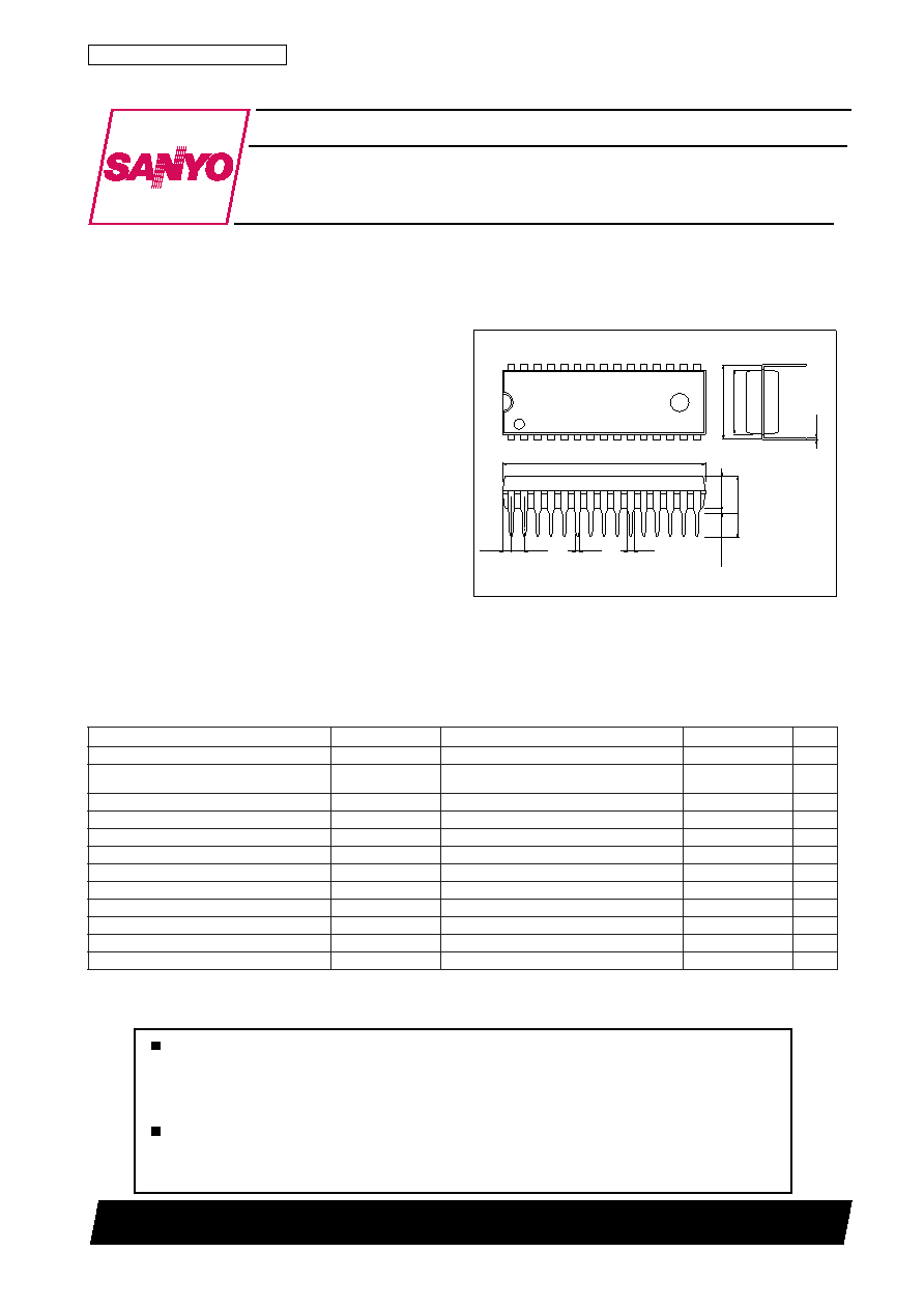
Package Dimensions
unit:mm
3061-DIP30S
[LA7953]
SANYO : DIP30S
Overview
The LA7953 Audio Controller is a single-chip, liner IC
featuring a built-in expansion circuit. The device also fea-
tures a 4-input 1-output audio switch, an acoustic mute, a
LINE-OUT output, and audio control functions for volume,
balance, bass and treble on-chip.
Excellent audio reproduction can be obtained using the right
channel expansion circuit.
The LA7953 operates on a single 12V power supply and is
available in 30-pin plastic DIPs.
Features
On-chip audio controller and audio switch facilitate de-
sign.
Audio controller for volume, balance, bass and treble.
4-input/1-output audio switch.
On-chip expansion circuit ensures excellent sound repro-
duction.
LINE-OUT output.
Acoustic mute.
Specifications
Maximum Ratings at Ta = 25C
1
15
30
16
1.15
1.78
27.2
0.25
10.16
8.6
0.48
0.95
4.25
3.2
4.95max
0.51min
r
e
t
e
m
a
r
a
Pl
o
b
m
y
Ss
n
o
i
t
i
d
n
o
Cs
g
n
i
t
a
Rt
i
n
U
e
g
a
t
l
o
v
y
l
p
u
s
m
u
m
i
x
a
MV C
C
x
a
m
4
1V
1
e
g
a
t
l
o
v
d
e
il
p
a
t
u
p
n
I
V1, 3, 5, 7, 9, 1
1 ,
3
1 , 5
1
x
a
m
V C
C
V
4
1
=2
1V
2
e
g
a
t
l
o
v
d
e
il
p
a
t
u
p
n
IV2, 4
1 , 6
1 , 0
3
x
a
mV C
C
V
4
1
=4
1V
3
e
g
a
t
l
o
v
d
e
il
p
a
t
u
p
n
IV4
V
,
x
a
m
6
x
a
mV C
C
V
4
1
=4
1V
e
g
a
t
l
o
v
d
e
il
p
a
t
u
p
n
i
e
t
u
MV8
x
a
mV C
C
V
4
1
=4
1V
e
g
a
t
l
o
v
d
e
il
p
a
t
u
p
n
i
n
o
i
s
n
a
p
x
EV 2
1
x
a
mV C
C
V
4
1
=4
1V
t
n
e
r
u
c
t
u
p
t
u
o
T
U
O
-
E
N
I
LI 7
1 , 9
2
x
a
m
5A
m
t
n
e
r
u
c
t
u
p
t
u
o
m
u
m
i
x
a
MI 3
2 , 5
2
x
a
m
5A
m
t
n
e
r
u
c
t
u
p
t
u
o
n
o
i
s
n
a
p
x
EI 9
1
x
a
m
5A
m
e
g
a
t
l
o
v
d
e
il
p
a
t
u
p
n
i
l
o
r
t
n
o
c
e
n
o
TV 0
2
V
,
x
a
m
8
2
x
a
mV C
C
V
4
1
=4
1V
e
g
a
t
l
o
v
d
e
il
p
a
r
e
t
li
f
s
a
BV 2
2
V
,
x
a
m
6
2
x
a
mV C
C
V
4
1
=4
1V
e
g
a
t
l
o
v
d
e
il
p
a
r
e
t
li
f
e
l
b
e
r
TV 1
2
V
,
x
a
m
7
2
x
a
mV C
C
V
4
1
=4
1V
Continued on next page.
相關(guān)PDF資料 |
PDF描述 |
|---|---|
| LA7953 | 2 CHANNEL(S), TONE CONTROL CIRCUIT, PDIP30 |
| LA79600GP | SPECIALTY CONSUMER CIRCUIT, QCC24 |
| LA79600GP | SPECIALTY CONSUMER CIRCUIT, QCC24 |
| LA7975 | 1-BAND, AUDIO TUNER, PSIP5 |
| LA7976 | 1-BAND, AUDIO TUNER, PSIP5 |
相關(guān)代理商/技術(shù)參數(shù) |
參數(shù)描述 |
|---|---|
| LA7954 | 制造商:SANYO 制造商全稱:Sanyo Semicon Device 功能描述:Video Switch for TV/VCR Use |
| LA7955 | 制造商:SANYO 制造商全稱:Sanyo Semicon Device 功能描述:Video Switch for TV/VCR Use |
| LA7956 | 制造商:Panasonic Industrial Company 功能描述:IC |
| LA7957 | 制造商:SANYO 制造商全稱:Sanyo Semicon Device 功能描述:Video Switch for TV/VCR Use |
| LA7958 | 制造商:SANYO 制造商全稱:Sanyo Semicon Device 功能描述:For TV, VTR Audio/Video Switch |
發(fā)布緊急采購(gòu),3分鐘左右您將得到回復(fù)。