- 您現(xiàn)在的位置:買賣IC網(wǎng) > PDF目錄299390 > L9326 PDF資料下載
參數(shù)資料
| 型號(hào): | L9326 |
| 文件頁數(shù): | 5/8頁 |
| 文件大?。?/td> | 136K |
| 代理商: | L9326 |
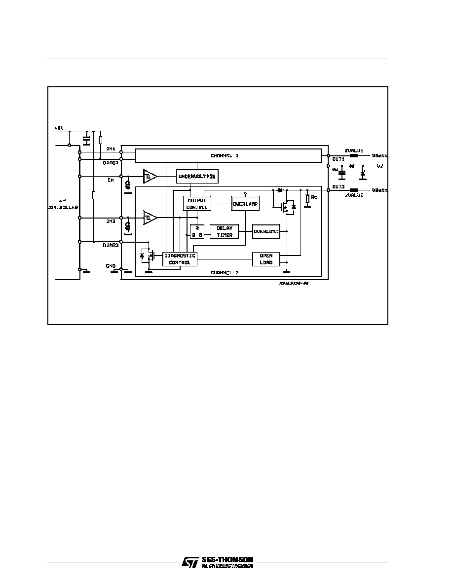
Figure 3: Application Circuit Diagram
CIRCUIT DESCRIPTION
The L9326 is a dual low side driver for inductive
loads like valves in automotive enviroment. The
device is enabled by a common CMOS compat-
ible ENABLE high signal. The internal pull down
resistances at the ENABLE and INPUT pins pro-
tect the device in open input conditions against
malfunctions. An output slope limitation for du/dt
is implemented to reduce the EMI. An integrated
active flyback voltage limitation clamps the output
voltage during the flyback phase to 50V.
Each driver is protected against short circuit con-
dition
1) the output will be disabled after a short
delay time tDOL to suppress spikes
2). This dis-
able is latched until a negative slope occure at the
correspondent input pin. The Thermal disable of
the output will be reseted if the junction tempera-
ture decreases below 160
°C.
For the real time error diagnosis the voltage and
the current of the output is compared with internal
fixed values VOu and IOu to recognize open load
(RL
≥ 20 K) in ON anf OFF conditions.
The diagnostic output level in connection with dif-
ferent ENABLE and INPUT conditions allows to
recognize four different fail states, under voltage,
over load, overtemp and open load.
The diagnostic output is also protected against
short circuit up to UDmax.
1) overstepeing the over load current thereshold IOo.
2) During the diagnostic overload delay switch-off time tDOL the output
current will be limited only by the RDSON of the output.
L9326
5/8
相關(guān)PDF資料 |
PDF描述 |
|---|---|
| L9335 | Injector Driver |
| L9336 | Injector Driver |
| L9337 | TRIPLE LOW SIDE DRIVER |
| LA1460 | 8 ELEMENT, SILICON, SIGNAL DIODE |
| LA3386-MQE7480 | T-1 SINGLE COLOR LED, AMBER, 3 mm |
相關(guān)代理商/技術(shù)參數(shù) |
參數(shù)描述 |
|---|---|
| L-932P3C | 制造商:Kingbright Corporation 功能描述: |
| L-9331 | 制造商:Ideal Industries Inc 功能描述:L-9331 |
| L9332 | 制造商:STMICROELECTRONICS 制造商全稱:STMicroelectronics 功能描述:Quad intelligent power low side switch |
| L9332-DIE1 | 制造商:STMICROELECTRONICS 制造商全稱:STMicroelectronics 功能描述:Quad intelligent power low side switch |
| L9333 | 制造商:STMICROELECTRONICS 制造商全稱:STMicroelectronics 功能描述:QUAD LOW SIDE DRIVER |
發(fā)布緊急采購,3分鐘左右您將得到回復(fù)。