- 您現(xiàn)在的位置:買賣IC網(wǎng) > PDF目錄367494 > L8567-44PLCC Telecommunication IC PDF資料下載
參數(shù)資料
| 型號: | L8567-44PLCC |
| 英文描述: | Telecommunication IC |
| 中文描述: | 通信集成電路 |
| 文件頁數(shù): | 14/42頁 |
| 文件大小: | 701K |
| 代理商: | L8567-44PLCC |
第1頁第2頁第3頁第4頁第5頁第6頁第7頁第8頁第9頁第10頁第11頁第12頁第13頁當(dāng)前第14頁第15頁第16頁第17頁第18頁第19頁第20頁第21頁第22頁第23頁第24頁第25頁第26頁第27頁第28頁第29頁第30頁第31頁第32頁第33頁第34頁第35頁第36頁第37頁第38頁第39頁第40頁第41頁第42頁
14
Lucent Technologies Inc.
Data Sheet
August 1999
People’s Republic of China Applications
L8567 SLIC for
Electrical Characteristics
(continued)
Transmit direction is tip/ring to 4-wire. Receive direction is 4-wire to tip/ring.
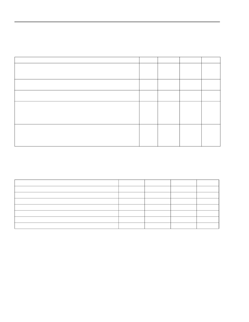
Table 7. ac Feed Characteristics
1. This parameter is not tested in production. It is guaranteed by design and device characterization.
Logic Interface
Table 8. Logic Inputs (B0, B1, EN, RD1I, RD2I, and RD3I) and Outputs (NSTAT and NTSD)
1. Unless otherwise specified, all logic voltages are referenced to DGND.
2. This parameter is not tested in production. It is guaranteed by design and device characterization.
Parameter
Min
Typ
Max
Unit
Total Harmonic Distortion—200 Hz to 4 kHz
1
:
Off-hook
On-hook
Transmit Gain, f = 1020 Hz (See Figure 11.); PT/PR to VTX
Transmit Gain
Receive Gain, f = 1020 Hz (See Figure 11.); RCVP/RCVN to PT/PR
Receive Gain
2-wire Idle-channel Noise (200
+ 680
||
0.1 μF termination):
Psophometric
1
C-message
3 kHz Flat
1
Transmit Idle-channel Noise:
Psophometric
1
C-message
3 kHz Flat
1
—
—
—
—
0.3
1.0
40.94
%
%
V/A
38.56
39.75
1.94
2
2.06
—
—
—
—
—
—
—
–77
12
20
dBmp
dBrnC
dBrn
—
—
—
—
—
—
–77
12
20
dBmp
dBrnC
dBrn
Parameter
1
Symbol
V
IH
V
IL
I
IN
V
OH
V
OL
I
OSS
C
OL
Min
2.4
0
—
Max
V
DDD
0.8
±
50
V
DD
0.4
35
50
Unit
V
V
μ
A
V
V
mA
pF
High-level Input Voltage
Low-level Input Voltage
Input Bias Current (high and low)
High-level Output Voltage (I
OUT
= –100
μ
A)
Low-level Output Voltage (I
OUT
= 180
μ
A)
Output Short-circuit Current (V
OUT
= V
DD
)
Output Load Capacitance
2
V
DD
– 1.5
0
1
0
相關(guān)PDF資料 |
PDF描述 |
|---|---|
| L8574D | CAP 15PF 50V 5% C0G SMD-0402 TR-7-PA SN100 |
| L8575 | Dual-Resistive,Low-Cost Subscriber Line Interface Circuit(SLIC) |
| L8576B | Dual Ringing SLIC |
| L8712(FECONLY) | IC TUBE FOR TO-220 508MM |
| L88R05_SERIES | |
相關(guān)代理商/技術(shù)參數(shù) |
參數(shù)描述 |
|---|---|
| L8574D | 制造商:AGERE 制造商全稱:AGERE 功能描述:L8574D Resistive Subscriber Line Interface Circuit(SLIC), Ring Relay,and Protector(SRP)for Long Loop and TR-57 Applications |
| L8575 | 制造商:Leviton Manufacturing Co 功能描述: |
| L8576B | 制造商:AGERE 制造商全稱:AGERE 功能描述:Dual Ringing SLIC |
| L8576BP | 制造商:Alcatel-Lucent 功能描述: 制造商:LUCENT 功能描述: |
| L85J250E | 制造商:Ohmite Mfg Co 功能描述: |
發(fā)布緊急采購,3分鐘左右您將得到回復(fù)。