- 您現(xiàn)在的位置:買賣IC網(wǎng) > PDF目錄384585 > L6598D (意法半導(dǎo)體) HIGH VOLTAGE RESONANT CONTROLLER PDF資料下載
參數(shù)資料
| 型號(hào): | L6598D |
| 廠商: | 意法半導(dǎo)體 |
| 英文描述: | HIGH VOLTAGE RESONANT CONTROLLER |
| 中文描述: | 高壓諧振控制器 |
| 文件頁數(shù): | 10/16頁 |
| 文件大小: | 114K |
| 代理商: | L6598D |
L6598
10/16
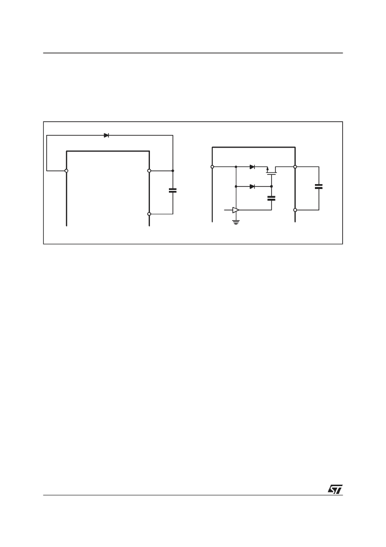
BootstrapSection
The supply of the high voltage section is obtained by means of a bootstrap circuitry. This solution normally re-
quires an high voltage fast recovery diode for charging the bootstrap capacitor (fig. 11a). In the L6568 a patent-
ed integrated structure, replaces this external diode. It is realised by means of a high voltage DMOS, driven
synchronously with the low side driver (LVG), with in series a diode, as shown in fig. 11b.
Figure 11. ootstrap driver
To drive the synchronised DMOS it is necessary a voltage higher than the supply voltage Vs. This voltage is
obtained by means of an internal charge pump (fig. 11b).
The diode connected in series to the DMOS has been added to avoid undesirable turn on of it. The introduction
of the diode prevents any current can flow from the V
boot
pin to the V
S
one in case that the supply is quickly
turned off when the internal capacitor of the pump is not fully discharged.
The bootstrap driver introduces a voltage drop during the recharging of the capacitor C
boot
(i.e. when the low
side driver is on), which increases with the frequency and with the size of the external power MOS. It is the sum
of the drop across the R
DSON
and of the diode threshold voltage. At low frequency this drop is very small and
can be neglected. Anyway increasing the frequency it must be taken in to account. In fact the drop, reducing
the amplitude of the driving signal, can significantly increase the R
DSON
of the external power MOS (and so the
dissipation).
To be considered that in resonant power supplies the current which flows in the power MOS decreases increas-
ing the switching frequency and generally the increases of R
DSON
is not a problem because power dissipation
is negligible. The following equation is useful to compute the drop on the bootstrap driver:
[8]
where Q
g
isthe gate charge of the external power MOS, R
dson
is the on resistance of the bootstrap DMOS, and
T
charge
is the time in which the bootstrap driver remains on (about the semiperiod of the switching frequency
minus the dead time). The typical resistance value of the bootstrap DMOS is 150 Ohm. For example using a
power MOS with a total gate charge of 30nC the drop on the bootstrap driver is about 3V, at a switching fre-
quency of 200kHz. In fact:
To summarise, if a significant drop on the bootstrap driver (at high switching frequency when large power MOS
are used) represents a problem, an external diode can be used, avoiding the drop on the R
DSON
of the DMOS.
V
S
V
BOOT
LVG
C
BOOT
V
OUT
V
S
V
BOOT
C
BOOT
V
OUT
D
BOOT
a
b
V
drop
I
ch
e
arg
R
dson
V
diode
V
drop
→
+
Q
T
ch
e
arg
-------------------
R
dson
V
diode
+
=
=
V
drop
2.23
μ
s
------------------
150
0.6V~2.6V
+
=
相關(guān)PDF資料 |
PDF描述 |
|---|---|
| L6599 | High-voltage resonant controller |
| L6599D | High-voltage resonant controller |
| L6599N | High-voltage resonant controller |
| L6599TR | High-voltage resonant controller |
| L6701 | 3 Phase Controller for VR10, VR9 and K8 CPUs |
相關(guān)代理商/技術(shù)參數(shù) |
參數(shù)描述 |
|---|---|
| L6598D013TR | 功能描述:PMIC 解決方案 High Volt Reson Cont RoHS:否 制造商:Texas Instruments 安裝風(fēng)格:SMD/SMT 封裝 / 箱體:QFN-24 封裝:Reel |
| L6598D016TR | 制造商:STMICROELECTRONICS 制造商全稱:STMicroelectronics 功能描述:High voltage resonant controller |
| L6599 | 制造商:STMICROELECTRONICS 制造商全稱:STMicroelectronics 功能描述:High-voltage resonant controller |
| L6599_0807 | 制造商:STMICROELECTRONICS 制造商全稱:STMicroelectronics 功能描述:High-voltage resonant controller |
| L6599A | 制造商:STMICROELECTRONICS 制造商全稱:STMicroelectronics 功能描述:Improved high-voltage resonant controller |
發(fā)布緊急采購,3分鐘左右您將得到回復(fù)。