- 您現(xiàn)在的位置:買賣IC網(wǎng) > PDF目錄1932 > KSZ9021RL (Micrel Inc)IC TXRX 10/100/1000 SGL 64LQFP PDF資料下載
參數(shù)資料
| 型號(hào): | KSZ9021RL |
| 廠商: | Micrel Inc |
| 文件頁(yè)數(shù): | 49/58頁(yè) |
| 文件大小: | 0K |
| 描述: | IC TXRX 10/100/1000 SGL 64LQFP |
| 標(biāo)準(zhǔn)包裝: | 160 |
| 類型: | 收發(fā)器 |
| 驅(qū)動(dòng)器/接收器數(shù): | 8/8 |
| 規(guī)程: | 千兆位以太網(wǎng) |
| 電源電壓: | 3.135 V ~ 3.465 V |
| 安裝類型: | 表面貼裝 |
| 封裝/外殼: | 64-LQFP 裸露焊盤 |
| 供應(yīng)商設(shè)備封裝: | 64-E-LQFP |
| 包裝: | 托盤 |
| 產(chǎn)品目錄頁(yè)面: | 1081 (CN2011-ZH PDF) |
| 其它名稱: | 576-3439 |
第1頁(yè)第2頁(yè)第3頁(yè)第4頁(yè)第5頁(yè)第6頁(yè)第7頁(yè)第8頁(yè)第9頁(yè)第10頁(yè)第11頁(yè)第12頁(yè)第13頁(yè)第14頁(yè)第15頁(yè)第16頁(yè)第17頁(yè)第18頁(yè)第19頁(yè)第20頁(yè)第21頁(yè)第22頁(yè)第23頁(yè)第24頁(yè)第25頁(yè)第26頁(yè)第27頁(yè)第28頁(yè)第29頁(yè)第30頁(yè)第31頁(yè)第32頁(yè)第33頁(yè)第34頁(yè)第35頁(yè)第36頁(yè)第37頁(yè)第38頁(yè)第39頁(yè)第40頁(yè)第41頁(yè)第42頁(yè)第43頁(yè)第44頁(yè)第45頁(yè)第46頁(yè)第47頁(yè)第48頁(yè)當(dāng)前第49頁(yè)第50頁(yè)第51頁(yè)第52頁(yè)第53頁(yè)第54頁(yè)第55頁(yè)第56頁(yè)第57頁(yè)第58頁(yè)
2010 Microchip Technology Inc.
DS22265A-page 53
MCP444X/446X
6.0
SERIAL INTERFACE (I2C)
The MCP44XX devices support the I2C serial protocol.
The MCP44XX I2C’s module operates in Slave mode
(does not generate the serial clock).
I2C interface signals are high-voltage tolerant.
The MCP44XX devices use the two-wire I2C serial
interface. This interface can operate in standard, fast or
High-Speed mode. A device that sends data onto the
bus is defined as transmitter, and a device receiving
data as receiver. The bus has to be controlled by a
master device which generates the serial clock (SCL),
controls the bus access and generates the START and
STOP conditions. The MCP44XX device works as
slave. Both master and slave can operate as
transmitter or receiver, but the master device
determines which mode is activated. Communication is
initiated by the master (microcontroller) which sends
the START bit, followed by the slave address byte. The
first byte transmitted is always the slave address byte,
which contains the device code, the address bits, and
the R/W bit.
Refer to the Phillips I2C document for more details of
the I2C specifications.
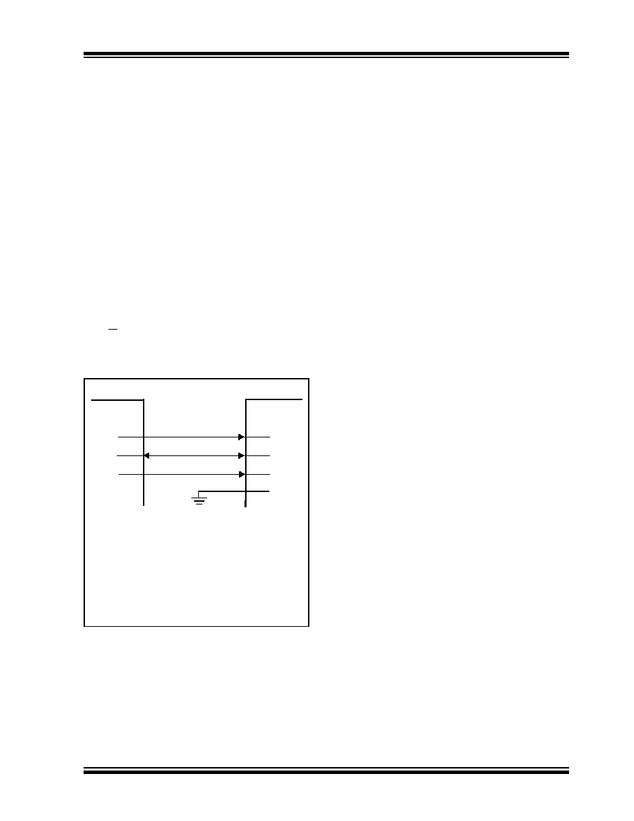
FIGURE 6-1:
Typical I2C Interface Block
Diagram.
6.1
Signal Descriptions
The I2C interface uses up to four pins (signals). These
are:
SDA (Serial Data)
SCL (Serial Clock)
A0 (Address 0 bit)
A1 (Address 1 bit)
6.1.1
SERIAL DATA (SDA)
The Serial Data (SDA) signal is the data signal of the
device. The value on this pin is latched on the rising
edge of the SCL signal when the signal is an input.
With the exception of the START and STOP conditions,
the high or low state of the SDA pin can only change
when the clock signal on the SCL pin is low. During the
high period of the clock, the SDA pin’s value (high or
low) must be stable. Changes in the SDA pin’s value
while the SCL pin is HIGH will be interpreted as a
START or a STOP condition.
6.1.2
SERIAL CLOCK (SCL)
The Serial Clock (SCL) signal is the clock signal of the
device. The rising edge of the SCL signal latches the
value on the SDA pin. The MCP44XX supports three
I2C interface clock modes:
Standard Mode: clock rates up to 100 kHz
Fast Mode: clock rates up to 400 kHz
High-Speed Mode (HS mode): clock rates up to
3.4 MHz
The MCP44XX will not stretch the clock signal (SCL)
since memory read access occur fast enough.
Depending on the clock rate mode, the interface will
display different characteristics.
6.1.3
THE ADDRESS BITS (A1:A0)
There are up to two hardware pins used to specify the
device address. The number of address pins is
determined by the part number.
Address 0 is multiplexed with the High Voltage
Command (HVC) function. So the state of A0 is latched
on the MCP4XXX’s POR/BOR event.
The state of the A1 pin should be static, that is they
should be tied high or tied low.
6.1.3.1
The High Voltage Command (HVC)
Signal
The High Voltage Command (HVC) signal is
multiplexed with Address 0 (A0) and is used to indicate
that the command, or sequence of commands, are in
the High Voltage mode. High Voltage commands allow
the device’s WiperLock Technology and write protect
features to be enabled and disabled.
The HVC pin has an internal resistor connection to the
MCP44XXs internal VDD signal.
SCL
MCP4XXX
SDA
HVC/A0 (2)
I/O (1)
Host
Controller
Typical I2C Interface Connections
Note 1:
If High voltage commands are desired,
some type of external circuitry needs to
be implemented.
2:
These pins have internal pull-ups. If
faster rise times are required, then
external pull-ups should be added.
3:
This pin could be tied high, low, or
connected to an I/O pin of the Host
Controller.
A1 (2, 3)
相關(guān)PDF資料 |
PDF描述 |
|---|---|
| KSZ9692PB | IC ARM9 PHY 5MBPS 400-PBGA |
| KSZ9692XPB | IC ARM9 PHY 5MBPS 400-PBGA |
| KXPC823ZT81B2T | IC MPU POWERQUICC 81MHZ 256-PBGA |
| KXPC8240RVV250E | IC MPU INTEGRATED 250MHZ 352TBGA |
| KXPC8260ZUIHBC | IC MPU POWERQUICC II 480-TBGA |
相關(guān)代理商/技術(shù)參數(shù) |
參數(shù)描述 |
|---|---|
| KSZ9021RL-EVAL | 制造商:Micrel Inc 功能描述:GIGABIT ETHERNET TRANSCEIVER W 制造商:Micrel Inc 功能描述:KIT EVALUATION FOR KSZ9021RL |
| KSZ9021RLI | 功能描述:以太網(wǎng) IC Gigabit Ethernet Transceiver with RGMII, I-Temp RoHS:否 制造商:Micrel 產(chǎn)品:Ethernet Switches 收發(fā)器數(shù)量:2 數(shù)據(jù)速率:10 Mb/s, 100 Mb/s 電源電壓-最大:1.25 V, 3.45 V 電源電壓-最小:1.15 V, 3.15 V 最大工作溫度:+ 85 C 封裝 / 箱體:QFN-64 封裝:Tray |
| KSZ9021RN | 功能描述:以太網(wǎng) IC Gigabit Ethernet Transceiver with RGMII, Lead Free RoHS:否 制造商:Micrel 產(chǎn)品:Ethernet Switches 收發(fā)器數(shù)量:2 數(shù)據(jù)速率:10 Mb/s, 100 Mb/s 電源電壓-最大:1.25 V, 3.45 V 電源電壓-最小:1.15 V, 3.15 V 最大工作溫度:+ 85 C 封裝 / 箱體:QFN-64 封裝:Tray |
| KSZ9021RN-EVAL | 功能描述:以太網(wǎng)開發(fā)工具 Gigabit Ethernet Transceiver with RGMII - Evaluation Board RoHS:否 制造商:Micrel 產(chǎn)品:Evaluation Boards 類型:Ethernet Transceivers 工具用于評(píng)估:KSZ8873RLL 接口類型:RMII 工作電源電壓: |
| KSZ9021RNI | 功能描述:以太網(wǎng) IC Gigabit Ethernet Transceiver with RGMII, I-Temp RoHS:否 制造商:Micrel 產(chǎn)品:Ethernet Switches 收發(fā)器數(shù)量:2 數(shù)據(jù)速率:10 Mb/s, 100 Mb/s 電源電壓-最大:1.25 V, 3.45 V 電源電壓-最小:1.15 V, 3.15 V 最大工作溫度:+ 85 C 封裝 / 箱體:QFN-64 封裝:Tray |
發(fā)布緊急采購(gòu),3分鐘左右您將得到回復(fù)。