- 您現在的位置:買賣IC網 > PDF目錄3945 > KMPC8379CVRALG (Freescale Semiconductor)IC MPU POWERQUICC II 689-PBGA PDF資料下載
參數資料
| 型號: | KMPC8379CVRALG |
| 廠商: | Freescale Semiconductor |
| 文件頁數: | 82/117頁 |
| 文件大小: | 0K |
| 描述: | IC MPU POWERQUICC II 689-PBGA |
| 標準包裝: | 2 |
| 系列: | MPC83xx |
| 處理器類型: | 32-位 MPC83xx PowerQUICC II Pro |
| 速度: | 667MHz |
| 電壓: | 1V |
| 安裝類型: | 表面貼裝 |
| 封裝/外殼: | 689-BBGA 裸露焊盤 |
| 供應商設備封裝: | 689-TEPBGA II(31x31) |
| 包裝: | 托盤 |
第1頁第2頁第3頁第4頁第5頁第6頁第7頁第8頁第9頁第10頁第11頁第12頁第13頁第14頁第15頁第16頁第17頁第18頁第19頁第20頁第21頁第22頁第23頁第24頁第25頁第26頁第27頁第28頁第29頁第30頁第31頁第32頁第33頁第34頁第35頁第36頁第37頁第38頁第39頁第40頁第41頁第42頁第43頁第44頁第45頁第46頁第47頁第48頁第49頁第50頁第51頁第52頁第53頁第54頁第55頁第56頁第57頁第58頁第59頁第60頁第61頁第62頁第63頁第64頁第65頁第66頁第67頁第68頁第69頁第70頁第71頁第72頁第73頁第74頁第75頁第76頁第77頁第78頁第79頁第80頁第81頁當前第82頁第83頁第84頁第85頁第86頁第87頁第88頁第89頁第90頁第91頁第92頁第93頁第94頁第95頁第96頁第97頁第98頁第99頁第100頁第101頁第102頁第103頁第104頁第105頁第106頁第107頁第108頁第109頁第110頁第111頁第112頁第113頁第114頁第115頁第116頁第117頁
MPC8379E PowerQUICC II Pro Processor Hardware Specifications, Rev. 8
Freescale Semiconductor
67
19.1
SPI DC Electrical Characteristics
This table provides the DC electrical characteristics for the device SPI.
19.2
SPI AC Timing Specifications
This table provides the SPI input and output AC timing specifications.
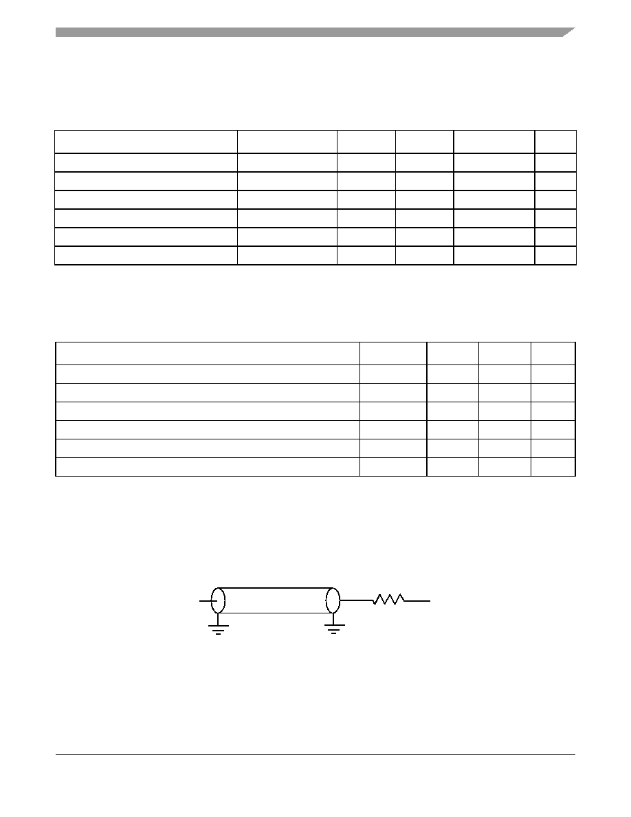
This figure provides the AC test load for the SPI.
Figure 45. SPI AC Test Load
These figures represent the AC timing from Table 67. Note that although the specifications generally
reference the rising edge of the clock, these AC timing diagrams also apply when the falling edge is the
active edge.
Table 66. SPI DC Electrical Characteristics
Parameter
Condition
Symbol
Min
Max
Unit
Input high voltage
—
VIH
2.0
OVDD + 0.3
V
Input low voltage
—
VIL
–0.3
0.8
V
Input current
—
IIN
—± 30
μA
Output high voltage
IOH = –8.0 mA
VOH
2.4
—
V
Output low voltage
IOL = 8.0 mA
VOL
—0.5
V
Output low voltage
IOL = 3.2 mA
VOL
—0.4
V
Table 67. SPI AC Timing Specifications
Parameter
Symbol1
Min
Max
Unit
SPI outputs—Master mode (internal clock) delay
tNIKHOV
0.5
6
ns
SPI outputs—Slave mode (external clock) delay
tNEKHOV
28
ns
SPI inputs—Master mode (internal clock) input setup time
tNIIVKH
4—
ns
SPI inputs—Master mode (internal clock) input hold time
tNIIXKH
0—
ns
SPI inputs—Slave mode (external clock) input setup time
tNEIVKH
4—
ns
SPI inputs—Slave mode (external clock) input hold time
tNEIXKH
2—
ns
Notes:
1. The symbols used for timing specifications follow the pattern of t(first two letters of functional block)(signal)(state) (reference)(state) for
inputs and t(first two letters of functional block)(reference)(state)(signal)(state) for outputs. For example, tNIKHOV symbolizes the internal
timing (NI) for the time SPICLK clock reference (K) goes to the high state (H) until outputs (O) are invalid (X).
2. Output specifications are measured from the 50% level of the rising edge of CLKIN to the 50% level of the signal. Timings
are measured at the pin. The maximum SPICLK input frequency is 66.666 MHz.
Output
Z0 = 50 Ω
OVDD/2
RL = 50 Ω
發(fā)布緊急采購,3分鐘左右您將得到回復。