- 您現(xiàn)在的位置:買賣IC網(wǎng) > PDF目錄374334 > KH205 (Fairchild Semiconductor Corporation) Overdrive-Protected Wideband Op Amp PDF資料下載
參數(shù)資料
| 型號: | KH205 |
| 廠商: | Fairchild Semiconductor Corporation |
| 英文描述: | Overdrive-Protected Wideband Op Amp |
| 中文描述: | 超速保護的寬帶運算放大器 |
| 文件頁數(shù): | 4/7頁 |
| 文件大小: | 125K |
| 代理商: | KH205 |
DATA SHEET
KH205
4
REV. 1A February 2001
Current Feedback Amplifiers
Some of the key features of current feedback technology
are:
I
Independence of AC bandwidth and voltage gain
I
Adjustable frequency response with feedback resistor
I
High slew rate
I
Fast settling
Current feedback operation can be described using a simple
equation. The voltage gain for a non-inverting or inverting
current feedback amplifier is approximated by Equation 1.
Equation 1
where:
I
A
v
is the closed loop DC voltage gain
I
R
f
is the feedback resistor
I
Z(j
ω
) is the CLC205
’
s open loop transimpedance
gain
ω
( )
I
is the loop gain
The denominator of Equation 1 is approximately equal to
1 at low frequencies. Near the -3dB corner frequency, the
interaction between R
f
and Z(j
ω
) dominates the circuit
performance. The value of the feedback resistor has a
large affect on the circuits performance. Increasing R
f
has the following affects:
I
Decreases loop gain
I
Decreases bandwidth
I
Reduces gain peaking
I
Lowers pulse response overshoot
I
Affects frequency response phase linearity
Overdrive Protection
Unlike most other high-speed op amps, the KH205 is not
damaged by saturation caused by overdriving input
signals (where V
in
x gain > max. V
o
). The KH205 self
limits the current at the inverting input when the output is
saturated (see the inverting input current self limit
specification); this ensures that the amplifier will not be
damaged due to excessive internal currents during overdrive.
For protection against input signals which would exceed
either the maximum differential or common mode input
voltage, the diode clamp circuits below may be used.
Figure 1: Diode Clamp Circuits for Common Mode
and Differential Mode Protection
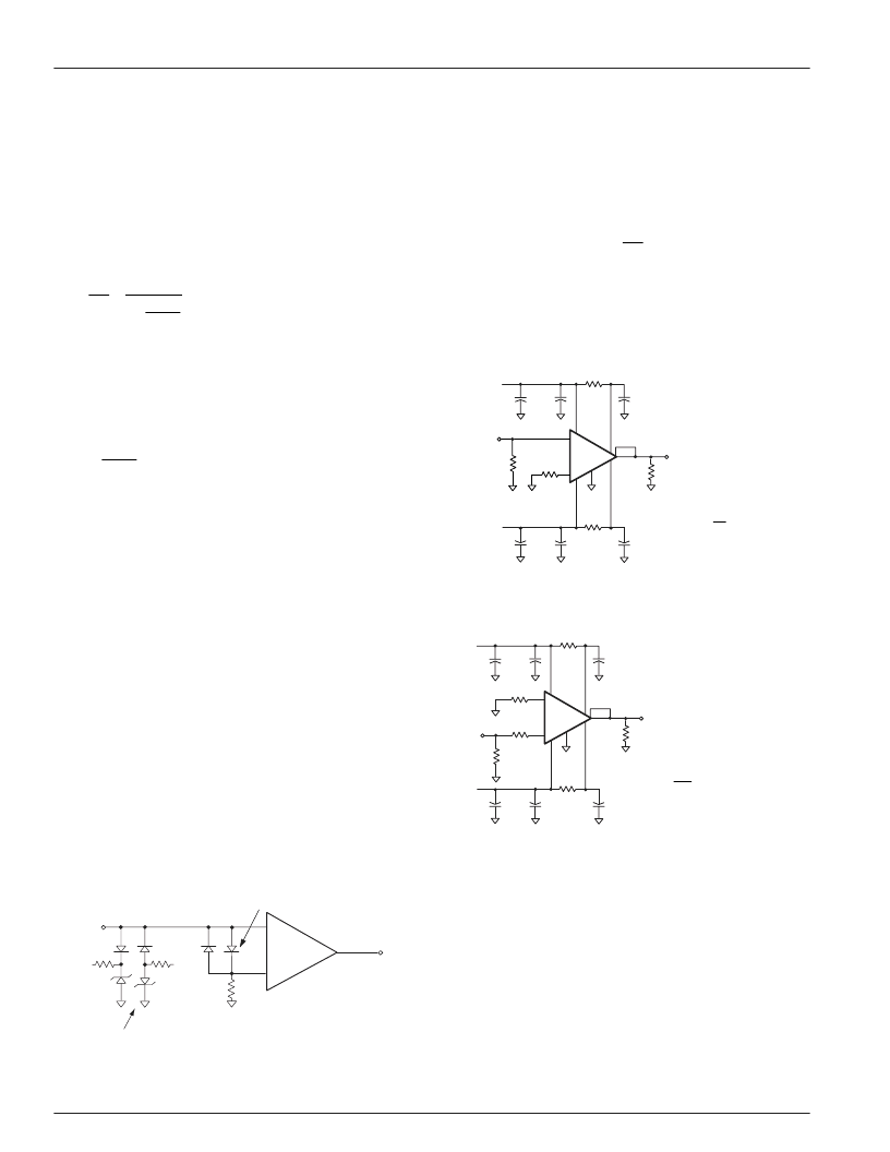
Short Circuit Protection
Damage caused by short circuits at the output may be
prevented by limiting the output current to safe levels.
The most simple current limit circuit calls for placing
resistors between the output stage collector supplies and
the output stage collectors (pins 12 and 10). The value of
this resistor is determined by:
where I
I
is the desired limit current and R
I
is the minimum
expected load resistance (0
for a short to ground).
Bypass capacitors of 0.01
μ
F on should be used on the
collectors as in Figures 2 and 3.
Figure 2: Recommended Non-Inverting Gain Circuit
Figure 3: Recommended Inverting Gain Circuit
A more sophisticated current limit circuit which provides
a limit current independent of R
I
is shown in Figure 4 on
page 5.
With the component values indicated, current limiting
occurs at 50mA. For other values of current limit (I
I
),
select R
C
to equal V
be
/l
I
.
emitter voltage drop of Q3 (or Q4) at a current of [2V
CC
–
1.4] / R
x
, where R
x
≤
[(2V
CC
–
1.4) / I
I
] B
min
.
Where V
be
is the base to
Also, B
min
is the minimum beta of Q1 (or Q2) at a current
of I
I
. Since the limit current depends on V
be
, which is
temperature
dependent,
likewise temperature dependent.
the
limit
current
is
differential protection
KH205
-
+
common mode
protection
R
g
+V
cc
V
in
V
o
-V
cc
R
V
I
R
C
C
I
I
=
33
+15V
.1
3.9
.01
Capactance in
μ
F
1
12
8
3,7
200
10
11
33
.01
.1
3.9
-15V
9
+
KH205
-
V
o
R
f
= 2000
(internal)
6
V
in
5
R
i
50
R
g
A
1
R
R
v
f
g
= +
33
+15V
.1
3.9
.01
Capactance in
μ
F
1
12
8
5
V
in
3,7
200
10
R
i
11
33
.01
.1
3.9
-15V
9
+
KH205
-
V
o
R
= 2000
(internal)
For Z
in
= 50
, select R
g
||R
i
= 50
6
50
R
g
A
-R
R
v
f
g
=
V
V
A
1
R
( )
ω
Z j
o
in
v
f
=
+
Z j
R
f
相關PDF資料 |
PDF描述 |
|---|---|
| KH206 | Overdrive-Protected Wideband Op Amp |
| KH207 | Low Distortion Wideband Op Amp |
| KH220 | Fast Settling Wideband Op Amp |
| KH231 | Fast Settling, Wideband Buffer/Amplifier (Av = 【1 to 【5) |
| KH232 | Low Distortion Wideband Op Amp |
相關代理商/技術參數(shù) |
參數(shù)描述 |
|---|---|
| KH205AI | 功能描述:運算放大器 - 運放 OP AMP WIDEBAND 170MHz 570mW 3MOHM RoHS:否 制造商:STMicroelectronics 通道數(shù)量:4 共模抑制比(最小值):63 dB 輸入補償電壓:1 mV 輸入偏流(最大值):10 pA 工作電源電壓:2.7 V to 5.5 V 安裝風格:SMD/SMT 封裝 / 箱體:QFN-16 轉(zhuǎn)換速度:0.89 V/us 關閉:No 輸出電流:55 mA 最大工作溫度:+ 125 C 封裝:Reel |
| KH205AK | 制造商:CADEKA 制造商全稱:CADEKA 功能描述:Overdrive-Protected Wideband Op Amp |
| KH205AM | 功能描述:運算放大器 - 運放 OP AMP WIDEBAND 170MHz 570mW 3MOHM RoHS:否 制造商:STMicroelectronics 通道數(shù)量:4 共模抑制比(最小值):63 dB 輸入補償電壓:1 mV 輸入偏流(最大值):10 pA 工作電源電壓:2.7 V to 5.5 V 安裝風格:SMD/SMT 封裝 / 箱體:QFN-16 轉(zhuǎn)換速度:0.89 V/us 關閉:No 輸出電流:55 mA 最大工作溫度:+ 125 C 封裝:Reel |
| KH205HXA | 制造商:CADEKA 制造商全稱:CADEKA 功能描述:Overdrive-Protected Wideband Op Amp |
| KH205HXC | 制造商:CADEKA 制造商全稱:CADEKA 功能描述:Overdrive-Protected Wideband Op Amp |
發(fā)布緊急采購,3分鐘左右您將得到回復。