- 您現(xiàn)在的位置:買賣IC網(wǎng) > PDF目錄374333 > KFN2G16Q2M-DEB5 (SAMSUNG SEMICONDUCTOR CO. LTD.) MuxOneNAND FLASH MEMORY PDF資料下載
參數(shù)資料
| 型號: | KFN2G16Q2M-DEB5 |
| 廠商: | SAMSUNG SEMICONDUCTOR CO. LTD. |
| 英文描述: | MuxOneNAND FLASH MEMORY |
| 中文描述: | MuxOneNAND閃存 |
| 文件頁數(shù): | 86/124頁 |
| 文件大小: | 1550K |
| 代理商: | KFN2G16Q2M-DEB5 |
第1頁第2頁第3頁第4頁第5頁第6頁第7頁第8頁第9頁第10頁第11頁第12頁第13頁第14頁第15頁第16頁第17頁第18頁第19頁第20頁第21頁第22頁第23頁第24頁第25頁第26頁第27頁第28頁第29頁第30頁第31頁第32頁第33頁第34頁第35頁第36頁第37頁第38頁第39頁第40頁第41頁第42頁第43頁第44頁第45頁第46頁第47頁第48頁第49頁第50頁第51頁第52頁第53頁第54頁第55頁第56頁第57頁第58頁第59頁第60頁第61頁第62頁第63頁第64頁第65頁第66頁第67頁第68頁第69頁第70頁第71頁第72頁第73頁第74頁第75頁第76頁第77頁第78頁第79頁第80頁第81頁第82頁第83頁第84頁第85頁當(dāng)前第86頁第87頁第88頁第89頁第90頁第91頁第92頁第93頁第94頁第95頁第96頁第97頁第98頁第99頁第100頁第101頁第102頁第103頁第104頁第105頁第106頁第107頁第108頁第109頁第110頁第111頁第112頁第113頁第114頁第115頁第116頁第117頁第118頁第119頁第120頁第121頁第122頁第123頁第124頁
MuxOneNAND1G(KFM1G16Q2M-DEB5)
MuxOneNAND2G(KFN2G16Q2M-DEB5)
FLASH MEMORY
86
An OTP Load Operation accesses the OTP area and transfers identified content from the OTP to the DataRAM on-chip buffer,
thus making the OTP contents available to the Host.
The OTP area is a separate part of the NAND Flash Array memory. It is accessed by issuing OTP Access command(65h) instead of
a Flash Block Address (FBA) command.
After being accessed with the OTP Access Command, the contents of OTP memory area are loaded using the same operations
as a normal load operation to the NAND Flash Array memory (see section 3.6 for more information).
To exit the OTP access mode following an OTP Load Operation, a Cold-, Warm-, Hot-, or NAND Flash Core Reset operation is per-
formed.
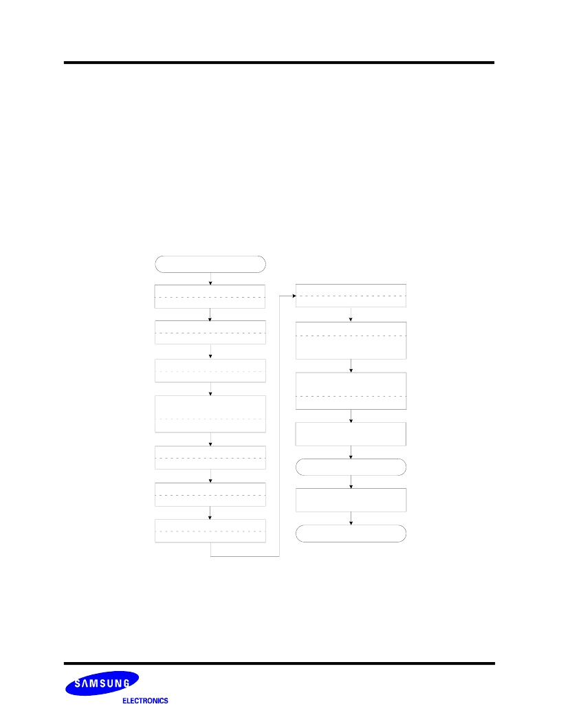
OTP Read Operation Flow Chart
Start
Wait for INT register
low to high transition
Add: F241h DQ[15]=INT
Write 0 to interrupt register
Add: F241h DQ=0000h
Write ’FPA, FSA’ of Flash
Add: F107h DQ=FPA, FSA
OTP Reading completed
Write ’Load’ Command
Add: F220h
DQ=0000h or 0013h
Wait for INT register
low to high transition
Add: F241h DQ[15]=INT
Write ’OTP Access’ Command
Add: F220h DQ=0065h
Write ’BSA, BSC’ of DataRAM
Add: F200h DQ=BSA, BSC
OTP Exit
Host reads data from
DataRAM
Note 1) FBA(NAND Flash Block Address) could be any address.
Do Cold/Warm/Hot
/NAND Flash Core Reset
* DFS is for DDP
Write ’DFS*, FBA’ of Flash
1)
Add: F100h DQ=DFS*’, FBA
Write 0 to interrupt register
Add: F241h DQ=0000h
Select DataRAM for DDP
Add: F101h DQ=DBS*
3.11.1 OTP Load Operation
相關(guān)PDF資料 |
PDF描述 |
|---|---|
| KFM1G16Q2M | MuxOneNAND FLASH MEMORY |
| KFM1G16Q2M-DEB5 | MuxOneNAND FLASH MEMORY |
| KFN1G16Q2M-DEB5 | MuxOneNAND FLASH MEMORY |
| KFM2G16Q2M-DEB5 | MuxOneNAND FLASH MEMORY |
| KFM1G16Q2M-DEB6 | MuxOneNAND FLASH MEMORY |
相關(guān)代理商/技術(shù)參數(shù) |
參數(shù)描述 |
|---|---|
| KFN2G16Q2M-DEB6 | 制造商:SAMSUNG 制造商全稱:Samsung semiconductor 功能描述:MuxOneNAND FLASH MEMORY |
| KFN2G16Q2M-DED5 | 制造商:SAMSUNG 制造商全稱:Samsung semiconductor 功能描述:MuxOneNAND FLASH MEMORY |
| KFN2G16Q2M-DED6 | 制造商:SAMSUNG 制造商全稱:Samsung semiconductor 功能描述:MuxOneNAND FLASH MEMORY |
| KFN305DL08 | 制造商:KAYNAR (ALCOA) 功能描述: |
| KFN305DL3 | 制造商:KAYNAR (ALCOA) 功能描述: |
發(fā)布緊急采購,3分鐘左右您將得到回復(fù)。