- 您現(xiàn)在的位置:買賣IC網(wǎng) > PDF目錄374282 > K4S641632E (SAMSUNG SEMICONDUCTOR CO. LTD.) Low Noise Precision Advanced LinCMOS(TM) Single Operational Amplifier 20-LCCC -55 to 125 PDF資料下載
參數(shù)資料
| 型號(hào): | K4S641632E |
| 廠商: | SAMSUNG SEMICONDUCTOR CO. LTD. |
| 英文描述: | Low Noise Precision Advanced LinCMOS(TM) Single Operational Amplifier 20-LCCC -55 to 125 |
| 中文描述: | 64Mbit SDRAM的 |
| 文件頁數(shù): | 6/10頁 |
| 文件大?。?/td> | 129K |
| 代理商: | K4S641632E |
K4S641632E
CMOS SDRAM
Rev.0.2 Sept. 2001
AC OPERATING TEST CONDITIONS
(V
DD
= 3.3V
±
0.3V, T
A
= 0 to 70
°
C)
Parameter
Value
Unit
AC input levels (Vih/Vil)
2.4/0.4
V
Input timing measurement reference level
1.4
V
Input rise and fall time
tr/tf = 1/1
ns
Output timing measurement reference level
1.4
V
Output load condition
See Fig. 2
3.3V
1200
870
Output
50pF
V
OH
(DC) = 2.4V, I
OH
= -2mA
V
OL
(DC) = 0.4V, I
OL
= 2mA
Vtt = 1.4V
50
Output
50pF
Z0 = 50
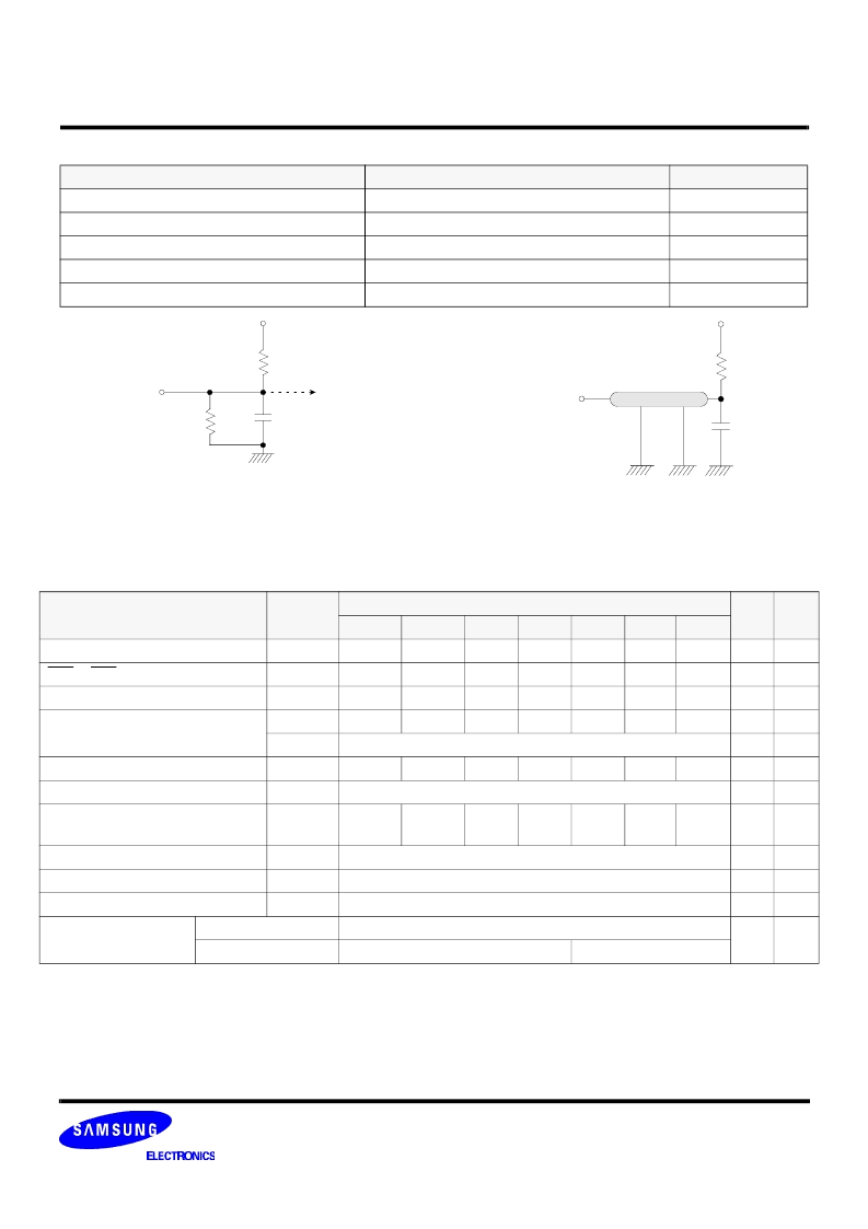
(Fig. 2) AC output load circuit
(Fig. 1) DC output load circuit
OPERATING AC PARAMETER
(AC operating conditions unless otherwise noted)
Notes :
Parameter
Symbol
Version
Unit
Note
-50
-55
-60
-70
-75
-1H
-1L
Row active to row active delay
t
RRD
(min)
10
11
12
14
15
20
20
ns
1
RAS to CAS delay
t
RCD
(min)
15
16.5
18
20
20
20
20
ns
1
Row precharge time
t
RP
(min)
15
16.5
18
20
20
20
20
ns
1
Row active time
t
RAS
(min)
38.5
38.5
42
49
45
50
50
ns
1
t
RAS
(max)
100
us
Row cycle time
t
RC
(min)
55
55
60
68
65
70
70
ns
1
Last data in to row precharge
t
RDL
(min)
2
CLK
2,5
Last data in to active delay
t
DAL
(min)
2CLK
+15ns
2CLK
+16.5ns
2CLK
+18ns
2CLK
+20ns
2CLK
+20ns
2CLK
+20ns
2CLK
+20ns
-
5
Last data in to new col. address Delay
t
CDL
(min)
1
CLK
2
Last data in to burst stop
t
BDL
(min)
1
CLK
2
Col. address to col. address delay
t
CCD
(min)
1
CLK
3
Number of valid output
data
CAS latency=3
2
ea
4
CAS latency=2
-
1
1. The DC/AC Test Output Load of K4S641632E-50/55/60 is 30pF.
2. The VDD condition of K4S641632E-50/55/60 is 3.135V~3.6V.
Notes :
1. The minimum number of clock cycles is determined by dividing the minimum time required with clock cycle time
and then rounding off to the next higher integer.
2. Minimum delay is required to complete write.
3. All parts allow every cycle column address change.
4. In case of row precharge interrupt, auto precharge and read burst stop.
5. In 100MHz and below 100MHz operating conditions, tRDL=1CLK and tDAL=1CLK + 20ns is also supported.
SAMSUNG recommends tRDL=2CLK and tDAL=2CLK + tRP.
相關(guān)PDF資料 |
PDF描述 |
|---|---|
| K4S641632E-TC1L | 64Mbit SDRAM |
| K4S641632F-TC1H | 64Mbit SDRAM 1M x 16Bit x 4 Banks Synchronous DRAM LVTTL |
| K4S641632F-TC50 | 64Mbit SDRAM 1M x 16Bit x 4 Banks Synchronous DRAM LVTTL |
| K4S641632F-TC55 | 64Mbit SDRAM 1M x 16Bit x 4 Banks Synchronous DRAM LVTTL |
| K4S641632F-TC60 | RF CONNECTOR; FME PLUG, CRIMP ATTACHMENT FOR RG58 |
相關(guān)代理商/技術(shù)參數(shù) |
參數(shù)描述 |
|---|---|
| K4S641632E-TC1H | 制造商:SAMSUNG 制造商全稱:Samsung semiconductor 功能描述:64Mbit SDRAM |
| K4S641632E-TC1H000 | 制造商:Samsung SDI 功能描述:DRAM Chip SDRAM 64M-Bit 4Mx16 3.3V 54-Pin TSOP-II Tray |
| K4S641632E-TC1L | 制造商:SAMSUNG 制造商全稱:Samsung semiconductor 功能描述:64Mbit SDRAM |
| K4S641632E-TC50 | 制造商:SAMSUNG 制造商全稱:Samsung semiconductor 功能描述:64Mbit SDRAM |
| K4S641632E-TC55 | 制造商:SAMSUNG 制造商全稱:Samsung semiconductor 功能描述:64Mbit SDRAM |
發(fā)布緊急采購,3分鐘左右您將得到回復(fù)。