- 您現(xiàn)在的位置:買賣IC網(wǎng) > PDF目錄374267 > K4H641638C-TLA2 (SAMSUNG SEMICONDUCTOR CO. LTD.) 128Mb DDR SDRAM PDF資料下載
參數(shù)資料
| 型號(hào): | K4H641638C-TLA2 |
| 廠商: | SAMSUNG SEMICONDUCTOR CO. LTD. |
| 英文描述: | 128Mb DDR SDRAM |
| 中文描述: | 128MB DDR SDRAM的 |
| 文件頁數(shù): | 40/53頁 |
| 文件大?。?/td> | 669K |
| 代理商: | K4H641638C-TLA2 |
第1頁第2頁第3頁第4頁第5頁第6頁第7頁第8頁第9頁第10頁第11頁第12頁第13頁第14頁第15頁第16頁第17頁第18頁第19頁第20頁第21頁第22頁第23頁第24頁第25頁第26頁第27頁第28頁第29頁第30頁第31頁第32頁第33頁第34頁第35頁第36頁第37頁第38頁第39頁當(dāng)前第40頁第41頁第42頁第43頁第44頁第45頁第46頁第47頁第48頁第49頁第50頁第51頁第52頁第53頁
- 40 -
REV. 1.0 November. 2. 2000
128Mb DDR SDRAM
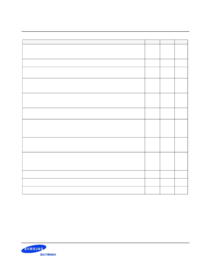
7.2 DDR SDRAM SPEC Items and Test Conditions
Typical case: VDD = 2.5V, T = 25’C
Worst case : VDD = 2.7V, T = 10’C
Conditions
Operating current - One bank Active-Precharge;
tRC=tRCmin;tCK=100Mhz for DDR200, 133Mhz for DDR266A & DDR266B;
DQ,DM and DQS inputs changing twice per clock cycle;
address and control inputs changing once per clock cycle
Operating current - One bank operation ;
One bank open, BL=4, Reads
- Refer to the following page for detailed test condition
Percharge power-down standby current;
All banks idle; power - down mode;
CKE = <VIL(max); tCK=100Mhz for DDR200, 133Mhz for DDR266A & DDR266B;
Vin = Vref for DQ,DQS and DM
Precharge Floating standby current;
CS# > =VIH(min);All banks idle;
CKE > = VIH(min); tCK=100Mhz for DDR200, 133Mhz for DDR266A & DDR266B;
Address and other control inputs changing once per clock cycle;
Vin = Vref for DQ,DQS and DM
Precharge Quiet standby current;
CS# > = VIH(min); All banks idle;
CKE > = VIH(min); tCK = 100Mhz for DDR200, 133Mhz for DDR266A & DDR266B;
Address and other control inputs stable with keeping >= VIH(min) or =<VIL(max);
Vin = Vref for DQ ,DQS and DM
Active power - down standby current ;
one bank active; power-down mode;
CKE=< VIL (max); tCK = 100Mhz for DDR200, 133Mhz for DDR266A & DDR266B;
Vin = Vref for DQ,DQS and DM
Active standby current;
CS# >= VIH(min); CKE>=VIH(min);
one bank active; active - precharge; tRC=tRASmax; tCK = 100Mhz for DDR200,
133Mhz for DDR266A & DDR266B; DQ, DQS and DM inputs changing twice
per clock cycle; address and other control inputs changing once
per clock cycle
Operating current - burst read;
Burst length = 2; reads; continguous burst;
One bank active; address and control inputs changing once per clock cycle;
CL=2 at tCK = 100Mhz for DDR200, CL=2 at tCK = 133Mhz for DDR266A, CL=2.5 at tCK =
133Mhz for DDR266B ; 50% of data changing at every burst; lout = 0 m A
Operating current - burst write;
Burst length = 2; writes; continuous burst;
One bank active address and control inputs changing once per clock cycle;
CL=2 at tCK = 100Mhz for DDR200, CL=2 at tCK = 133Mhz for DDR266A,
CL=2.5 at tCK = 133Mhz for DDR266B ; DQ, DM and DQS inputs changing twice
per clock cycle, 50% of input data changing at every burst
Auto refresh current;
tRC = tRFC(min) - 8*tCK for DDR200 at 100Mhz,
10*tCK for DDR266A & DDR266B at 133Mhz; distributed refresh
Self refresh current;
CKE =< 0.2V; External clock should be on;
tCK = 100Mhz for DDR200, 133Mhz for DDR266A & DDR266B
Orerating current - Four bank operation ;
Four bank interleaving with BL=4
-Refer to the following page for detailed test condition
Symbol
IDD0
Typical
Worst
-
-
IDD1
-
-
IDD2P
-
-
IDD2F
-
-
IDD2Q
-
-
IDD3P
-
-
IDD3N
-
-
IDD4R
-
-
IDD4W
-
-
IDD5
-
-
IDD6
-
-
IDD7
-
-
相關(guān)PDF資料 |
PDF描述 |
|---|---|
| K4H641638C-TLB0 | 128Mb DDR SDRAM |
| K4H641638D-TCA0 | 128Mb DDR SDRAM |
| K4H641638D-TCA2 | 128Mb DDR SDRAM |
| K4H641638D-TCB0 | 128Mb DDR SDRAM |
| K4H641638D-TLA0 | 128Mb DDR SDRAM |
相關(guān)代理商/技術(shù)參數(shù) |
參數(shù)描述 |
|---|---|
| K4H641638C-TLB0 | 制造商:SAMSUNG 制造商全稱:Samsung semiconductor 功能描述:128Mb DDR SDRAM |
| K4H641638D-TCA0 | 制造商:SAMSUNG 制造商全稱:Samsung semiconductor 功能描述:128Mb DDR SDRAM |
| K4H641638D-TCA2 | 制造商:SAMSUNG 制造商全稱:Samsung semiconductor 功能描述:128Mb DDR SDRAM |
| K4H641638D-TCB0 | 制造商:SAMSUNG 制造商全稱:Samsung semiconductor 功能描述:128Mb DDR SDRAM |
| K4H641638D-TLA0 | 制造商:SAMSUNG 制造商全稱:Samsung semiconductor 功能描述:128Mb DDR SDRAM |
發(fā)布緊急采購,3分鐘左右您將得到回復(fù)。