- 您現(xiàn)在的位置:買賣IC網(wǎng) > PDF目錄374275 > K4H560438E-TCAA (SAMSUNG SEMICONDUCTOR CO. LTD.) 256Mb E-die DDR SDRAM Specification 66 TSOP-II PDF資料下載
參數(shù)資料
| 型號: | K4H560438E-TCAA |
| 廠商: | SAMSUNG SEMICONDUCTOR CO. LTD. |
| 英文描述: | 256Mb E-die DDR SDRAM Specification 66 TSOP-II |
| 中文描述: | 256Mb的電子芯片DDR SDRAM內(nèi)存規(guī)格66 TSOP-II |
| 文件頁數(shù): | 16/26頁 |
| 文件大?。?/td> | 291K |
| 代理商: | K4H560438E-TCAA |
第1頁第2頁第3頁第4頁第5頁第6頁第7頁第8頁第9頁第10頁第11頁第12頁第13頁第14頁第15頁當(dāng)前第16頁第17頁第18頁第19頁第20頁第21頁第22頁第23頁第24頁第25頁第26頁
- 16 -
K4H560838D
DDR SDRAM
Rev. 2.2 Mar. ’03
Notes 1. Includes
±
25mV margin for DC offset on V
REF
, and a combined total of
±
50mV margin for all AC noise and DC offset on
V
REF
, bandwidth limited to 20MHz. The DRAM must accommodate DRAM current spikes on V
REF
and internal DRAM noise
coupled TO V
REF
, both of which may result in V
REF
noise. V
REF
should be de-coupled with an inductance of
≤
3nH.
2. V
TT
is not applied directly to the device. V
TT
is a system supply for signal termination resistors, is expected to be set equal to
V
REF
, and must track variations in the DC level of V
REF
3. V
ID
is the magnitude of the difference between the input level on CK and the input level on CK.
4. These parameters should be tested at the pin on actual components and may be checked at either the pin or the pad in
simulation. The AC and DC input specifications are relative to a VREF envelop that has been bandwidth limited to 200MHZ.
5. The value of V
IX
is expected to equal 0.5*V
DDQ
of the transmitting device and must track variations in the dc level of the same.
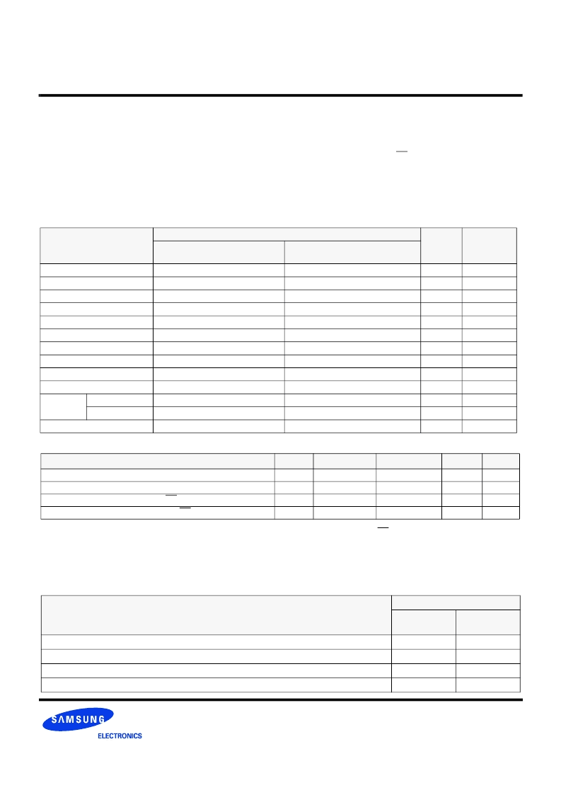
DDR SDRAM IDD spec table
AC Operating Conditions
Parameter/Condition
Symbol
Min
Max
Unit
Note
Input High (Logic 1) Voltage, DQ, DQS and DM signals
Input Low (Logic 0) Voltage, DQ, DQS and DM signals.
Input Differential Voltage, CK and CK inputs
Input Crossing Point Voltage, CK and CK inputs
VIH(AC)
VIL(AC)
VID(AC)
VIX(AC)
VREF + 0.31
V
V
V
V
3
3
1
2
VREF - 0.31
VDDQ+0.6
0.5*VDDQ+0.2
0.7
0.5*VDDQ-0.2
Note 1. VID is the magnitude of the difference between the input level on CK and the input on CK.
2. The value of V
IX
is expected to equal 0.5*V
DDQ
of the transmitting device and must track variations in the DC level of the same.
3. These parameters should be tested at the pim on actual components and may be checked at either the pin or the pad in simu
lation. the AC and DC input specificatims are refation to a Vref envelope that has been bandwidth limited 20MHz.
(V
DD
=2.7V, T
= 10
°
C
)
Parameter
Specification
Address &
Control pins
1.6 V
1.6 V
4.5 V-ns
4.5 V-ns
Data pins
Maximum peak amplitude allowed for overshoot
Maximum peak amplitude allowed for undershoot
The area between the overshoot signal and VDD must be less than or equal to
The area between the undershoot signal and GND must be less than or equal to
1.2V
1.2V
2.5 V-ns
2.5 V-ns
Overshoot/Undershoot specification
Symbol
32Mx8
Unit
Notes
K4H560838D-GC(L)B3
(DDR333)
90
120
3
25
20
35
55
170
170
3
1.5
325
K4H560838D-GC(L)A2, B0
(DDR266A/B)
80
110
3
20
18
30
140
140
165
3
1.5
280
IDD0
IDD1
IDD2P
IDD2F
IDD2Q
IDD3P
IDD3N
IDD4R
IDD4W
IDD5
mA
mA
mA
mA
mA
mA
mA
mA
mA
mA
mA
mA
mA
IDD6
Normal
Low power
IDD7A
Optional
相關(guān)PDF資料 |
PDF描述 |
|---|---|
| K4H560438E-TCB0 | Dual Micropower Precision Low-Voltage Operational Amplifier 8-SOIC -40 to 85 |
| K4H560438E-TCB3 | 256Mb E-die DDR SDRAM Specification 66 TSOP-II |
| K4H560438E-TLA0 | 128Mb DDR SDRAM |
| K4H560438E-TLA2 | Dual Micropower Precision Low-Voltage Operational Amplifier 8-PDIP -40 to 85 |
| K4H560438E-TLAA | Dual Micropower Precision Low-Voltage Operational Amplifier 8-SOIC -55 to 125 |
相關(guān)代理商/技術(shù)參數(shù) |
參數(shù)描述 |
|---|---|
| K4H560438E-TCB0 | 制造商:Samsung Semiconductor 功能描述:DRAM Chip DDR SDRAM 256M-Bit 64Mx4 2.5V 66-Pin TSOP-II T/R |
| K4H560438E-TCB3 | 制造商:SAMSUNG 制造商全稱:Samsung semiconductor 功能描述:256Mb E-die DDR SDRAM Specification 66 TSOP-II |
| K4H560438E-TLA0 | 制造商:SAMSUNG 制造商全稱:Samsung semiconductor 功能描述:128Mb DDR SDRAM |
| K4H560438E-TLA2 | 制造商:SAMSUNG 制造商全稱:Samsung semiconductor 功能描述:256Mb E-die DDR SDRAM Specification 66 TSOP-II |
| K4H560438E-TLAA | 制造商:SAMSUNG 制造商全稱:Samsung semiconductor 功能描述:256Mb E-die DDR SDRAM Specification 66 TSOP-II |
發(fā)布緊急采購,3分鐘左右您將得到回復(fù)。