- 您現(xiàn)在的位置:買賣IC網(wǎng) > PDF目錄374266 > K4H280838E-TCA2 (SAMSUNG SEMICONDUCTOR CO. LTD.) 128Mb DDR SDRAM PDF資料下載
參數(shù)資料
| 型號(hào): | K4H280838E-TCA2 |
| 廠商: | SAMSUNG SEMICONDUCTOR CO. LTD. |
| 英文描述: | 128Mb DDR SDRAM |
| 中文描述: | 128MB DDR SDRAM的 |
| 文件頁數(shù): | 39/53頁 |
| 文件大小: | 669K |
| 代理商: | K4H280838E-TCA2 |
第1頁第2頁第3頁第4頁第5頁第6頁第7頁第8頁第9頁第10頁第11頁第12頁第13頁第14頁第15頁第16頁第17頁第18頁第19頁第20頁第21頁第22頁第23頁第24頁第25頁第26頁第27頁第28頁第29頁第30頁第31頁第32頁第33頁第34頁第35頁第36頁第37頁第38頁當(dāng)前第39頁第40頁第41頁第42頁第43頁第44頁第45頁第46頁第47頁第48頁第49頁第50頁第51頁第52頁第53頁
- 39 -
REV. 1.0 November. 2. 2000
128Mb DDR SDRAM
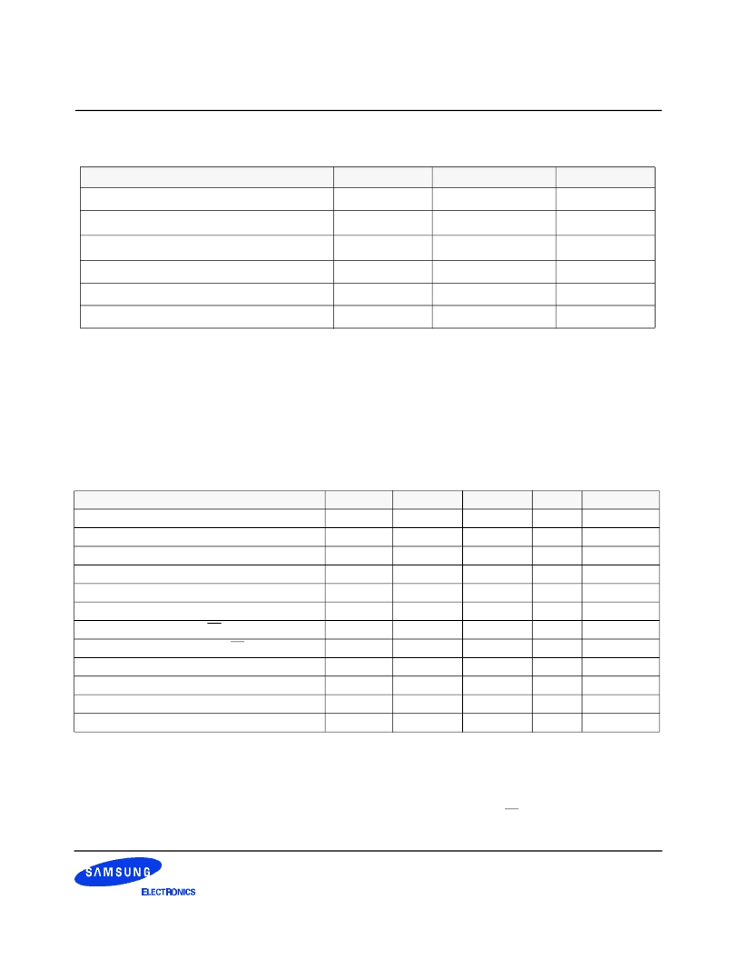
6. Absolute Maximum Rating
7. DC Operating Conditions & Specifications
7.1 DC Operating Conditions
Parameter
Symbol
Value
Unit
Voltage on any pin relative to V
SS
V
IN
, V
OUT
-0.5 ~ 3.6
V
Voltage on V
DD
supply relative to V
SS
V
DD
, V
DDQ
-1.0 ~ 3.6
V
Voltage on V
DDQ
supply relative to V
SS
V
DDQ
-0.5 ~ 3.6
V
Storage temperature
T
STG
-55 ~ +150
°
C
Power dissipation
P
D
1.0
W
Short circuit current
I
OS
50
mA
Note :
Permanent device damage may occur if ABSOLUTE MAXIMUM RATINGS are exceeded.
Functional operation should be restricted to recommend operation condition.
Exposure to higher than recommended voltage for extended periods of time could affect device reliability
Recommended operating conditions(Voltage referenced to V
SS
=0V, T
A
=0 to 70
°
C)
Parameter
Symbol
Min
Max
Unit
Note
Supply voltage(for device with a nominal V
DD
of 2.5V)
V
DD
2.3
2.7
I/O Supply voltage
V
DDQ
2.3
2.7
V
I/O Reference voltage
V
REF
0.49*VDDQ
0.51*VDDQ
V
1
I/O Termination voltage(system)
V
TT
V
REF
-0.04
V
REF
+0.04
V
2
Input logic high voltage
V
IH
(DC)
V
REF
+0.15
V
DDQ
+0.3
V
Input logic low voltage
V
IL
(DC)
-0.3
V
REF
-0.15
V
Input Voltage Level, CK and CK inputs
V
IN
(DC)
-0.3
V
DDQ
+0.3
V
Input Differential Voltage, CK and CK inputs
V
ID
(DC)
0.3
V
DDQ
+0.6
V
3
Input leakage current
I
I
-2
2
uA
Output leakage current
I
OZ
-5
5
uA
Output High Current (V
OUT
= 1.95V)
I
OH
-16.8
mA
Output Low Current (V
OUT
= 0.35V)
I
OL
16.8
mA
Notes 1. V
REF
is expected to be equal to 0.5*V
DDQ
of the transmitting device, and to track variations in the DC level of the same. Peak-to-
peak noise on V
REF
may not exceed 2% of the DC value
2.V
TT
is not applied directly to the device. V
TT
is a system supply for signal termination resistors, is expected to be set equal to
V
REF
, and must track variations in the DC level of V
REF
3. V
ID
is the magnitude of the difference between the input level on CK and the input level on CK.
Table 10. Absolute maximum ratings
Table 11. DC operating condition
相關(guān)PDF資料 |
PDF描述 |
|---|---|
| K4H280838E-TCB0 | 128Mb DDR SDRAM |
| K4H280838E-TLA0 | 128Mb DDR SDRAM |
| K4H280838E-TLA2 | 128Mb DDR SDRAM |
| K4H280838E-TLB0 | 128Mb DDR SDRAM |
| K4H280838F-UCA2 | 128Mb F-die DDR SDRAM Specification 66 TSOP-II with Pb-Free (RoHS compliant) |
相關(guān)代理商/技術(shù)參數(shù) |
參數(shù)描述 |
|---|---|
| K4H280838E-TCB0 | 制造商:Samsung Electro-Mechanics 功能描述:16M X 8 DDR DRAM, 0.75 ns, PDSO66 |
| K4H280838E-TLA0 | 制造商:SAMSUNG 制造商全稱:Samsung semiconductor 功能描述:128Mb DDR SDRAM |
| K4H280838E-TLA2 | 制造商:SAMSUNG 制造商全稱:Samsung semiconductor 功能描述:128Mb DDR SDRAM |
| K4H280838E-TLB0 | 制造商:SAMSUNG 制造商全稱:Samsung semiconductor 功能描述:128Mb DDR SDRAM |
| K4H280838F-TC/LA2 | 制造商:SAMSUNG 制造商全稱:Samsung semiconductor 功能描述:128Mb F-die DDR SDRAM Specification |
發(fā)布緊急采購,3分鐘左右您將得到回復(fù)。