- 您現在的位置:買賣IC網 > PDF目錄45382 > IT80C32E-12:RD (ATMEL CORP) 8-BIT, 12 MHz, MICROCONTROLLER, PQFP44 PDF資料下載
參數資料
| 型號: | IT80C32E-12:RD |
| 廠商: | ATMEL CORP |
| 元件分類: | 微控制器/微處理器 |
| 英文描述: | 8-BIT, 12 MHz, MICROCONTROLLER, PQFP44 |
| 封裝: | 1 MM HEIGHT, TQFP-44 |
| 文件頁數: | 88/226頁 |
| 文件大小: | 3676K |
第1頁第2頁第3頁第4頁第5頁第6頁第7頁第8頁第9頁第10頁第11頁第12頁第13頁第14頁第15頁第16頁第17頁第18頁第19頁第20頁第21頁第22頁第23頁第24頁第25頁第26頁第27頁第28頁第29頁第30頁第31頁第32頁第33頁第34頁第35頁第36頁第37頁第38頁第39頁第40頁第41頁第42頁第43頁第44頁第45頁第46頁第47頁第48頁第49頁第50頁第51頁第52頁第53頁第54頁第55頁第56頁第57頁第58頁第59頁第60頁第61頁第62頁第63頁第64頁第65頁第66頁第67頁第68頁第69頁第70頁第71頁第72頁第73頁第74頁第75頁第76頁第77頁第78頁第79頁第80頁第81頁第82頁第83頁第84頁第85頁第86頁第87頁當前第88頁第89頁第90頁第91頁第92頁第93頁第94頁第95頁第96頁第97頁第98頁第99頁第100頁第101頁第102頁第103頁第104頁第105頁第106頁第107頁第108頁第109頁第110頁第111頁第112頁第113頁第114頁第115頁第116頁第117頁第118頁第119頁第120頁第121頁第122頁第123頁第124頁第125頁第126頁第127頁第128頁第129頁第130頁第131頁第132頁第133頁第134頁第135頁第136頁第137頁第138頁第139頁第140頁第141頁第142頁第143頁第144頁第145頁第146頁第147頁第148頁第149頁第150頁第151頁第152頁第153頁第154頁第155頁第156頁第157頁第158頁第159頁第160頁第161頁第162頁第163頁第164頁第165頁第166頁第167頁第168頁第169頁第170頁第171頁第172頁第173頁第174頁第175頁第176頁第177頁第178頁第179頁第180頁第181頁第182頁第183頁第184頁第185頁第186頁第187頁第188頁第189頁第190頁第191頁第192頁第193頁第194頁第195頁第196頁第197頁第198頁第199頁第200頁第201頁第202頁第203頁第204頁第205頁第206頁第207頁第208頁第209頁第210頁第211頁第212頁第213頁第214頁第215頁第216頁第217頁第218頁第219頁第220頁第221頁第222頁第223頁第224頁第225頁第226頁
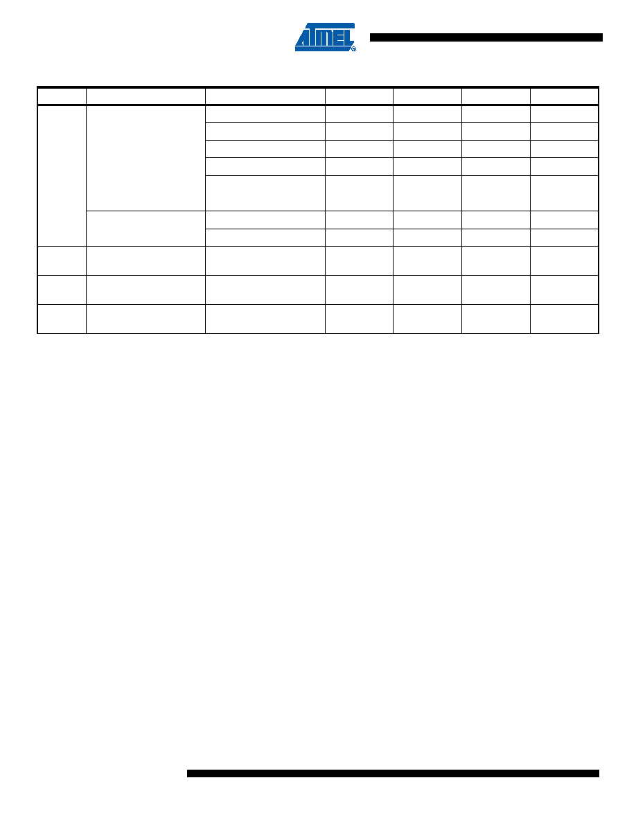
178
2543L–AVR–08/10
ATtiny2313
Notes: 1. All DC Characteristics contained in this data sheet are based on simulation and characterization of other AVR microcon-
trollers manufactured in the same process technology. These values are preliminary values representing design targets, and
will be updated after characterization of actual silicon.
2. Typical values at +25
°C.
3. “Max” means the highest value where the pin is guaranteed to be read as low.
4. “Min” means the lowest value where the pin is guaranteed to be read as high.
5. Although each I/O port can sink more than the test conditions (10 mA at VCC = 5V, 5 mA at VCC = 3V) under steady state
conditions (non-transient), the following must be observed:
1] The sum of all IOL, for all ports, should not exceed 60 mA.
If IOL exceeds the test condition, VOL may exceed the related specification. Pins are not guaranteed to sink current greater
than the listed test condition.
6. Although each I/O port can source more than the test conditions (10 mA at VCC = 5V, 5 mA at VCC = 3V) under steady state
conditions (non-transient), the following must be observed:
1] The sum of all IOH, for all ports, should not exceed 60 mA.
If IOH exceeds the test condition, VOH may exceed the related specification. Pins are not guaranteed to source current
greater than the listed test condition.
ICC
Power Supply Current
Active 1MHz, VCC = 2V
0.35
mA
Active 4MHz, VCC = 3V
2
mA
Active 8MHz, VCC = 5V
6
mA
Idle 1MHz, VCC = 2V
0.08
0.2
mA
Idle 4MHz, VCC = 3V
0.41
1
mA
Idle 8MHz, VCC = 5V
1.6
3
mA
Power-down mode
WDT enabled, VCC = 3V
< 3
6
A
WDT disabled, VCC = 3V
< 0.5
2
A
VACIO
Analog Comparator
Input Offset Voltage
VCC = 5V
Vin = VCC/2
< 10
40
mV
IACLK
Analog Comparator
Input Leakage Current
VCC = 5V
Vin = VCC/2
-50
50
nA
tACPD
Analog Comparator
Propagation Delay
VCC = 2.7V
VCC = 5.0V
750
500
ns
TA = -40°C to +85°C, VCC = 1.8V to 5.5V (unless otherwise noted)
(1) (Continued)
Symbol
Parameter
Condition
Min.
Typ.(2)
Max.
Units
相關PDF資料 |
PDF描述 |
|---|---|
| IF180C52CXXX-L16D | 8-BIT, MROM, 16 MHz, MICROCONTROLLER, PQFP44 |
| MC80C32-30:D | 8-BIT, 30 MHz, MICROCONTROLLER, CDIP40 |
| MT80C51T-30R | 8-BIT, MROM, 30 MHz, MICROCONTROLLER, PQFP44 |
| MD80C32E-12P883D | 8-BIT, 12 MHz, MICROCONTROLLER, CDIP40 |
| MD80C32E-12SBD | 8-BIT, 12 MHz, MICROCONTROLLER, CDIP40 |
相關代理商/技術參數 |
參數描述 |
|---|---|
| IT80C32-L16 | 制造商:未知廠家 制造商全稱:未知廠家 功能描述:8-Bit Microcontroller |
| IT80C32-L16R | 制造商:未知廠家 制造商全稱:未知廠家 功能描述:8-Bit Microcontroller |
| IT80C51-12 | 制造商:未知廠家 制造商全稱:未知廠家 功能描述:8-Bit Microcontroller |
| IT80C51-16 | 制造商:未知廠家 制造商全稱:未知廠家 功能描述:8-Bit Microcontroller |
| IT80C51-20 | 制造商:未知廠家 制造商全稱:未知廠家 功能描述:8-Bit Microcontroller |
發(fā)布緊急采購,3分鐘左右您將得到回復。