- 您現(xiàn)在的位置:買(mǎi)賣(mài)IC網(wǎng) > PDF目錄19841 > ISPLSI 2032A-150LJN44 (Lattice Semiconductor Corporation)IC PLD ISP 32I/O 5.5NS 44PLCC PDF資料下載
參數(shù)資料
| 型號(hào): | ISPLSI 2032A-150LJN44 |
| 廠商: | Lattice Semiconductor Corporation |
| 文件頁(yè)數(shù): | 9/16頁(yè) |
| 文件大小: | 0K |
| 描述: | IC PLD ISP 32I/O 5.5NS 44PLCC |
| 標(biāo)準(zhǔn)包裝: | 26 |
| 系列: | ispLSI® 2000A |
| 可編程類(lèi)型: | 系統(tǒng)內(nèi)可編程 |
| 最大延遲時(shí)間 tpd(1): | 5.5ns |
| 電壓電源 - 內(nèi)部: | 4.75 V ~ 5.25 V |
| 邏輯元件/邏輯塊數(shù)目: | 8 |
| 宏單元數(shù): | 32 |
| 門(mén)數(shù): | 1000 |
| 輸入/輸出數(shù): | 32 |
| 工作溫度: | 0°C ~ 70°C |
| 安裝類(lèi)型: | 表面貼裝 |
| 封裝/外殼: | 44-LCC(J 形引線) |
| 供應(yīng)商設(shè)備封裝: | 44-PLCC(16.58x16.58) |
| 包裝: | 管件 |
| 其它名稱(chēng): | ISPLSI2032A-150LJN44 |
第1頁(yè)第2頁(yè)第3頁(yè)第4頁(yè)第5頁(yè)第6頁(yè)第7頁(yè)第8頁(yè)當(dāng)前第9頁(yè)第10頁(yè)第11頁(yè)第12頁(yè)第13頁(yè)第14頁(yè)第15頁(yè)第16頁(yè)
Specifications ispLSI 2032/A
2
USE
ispLSI
2032E
FOR
NEW
DESIGNS
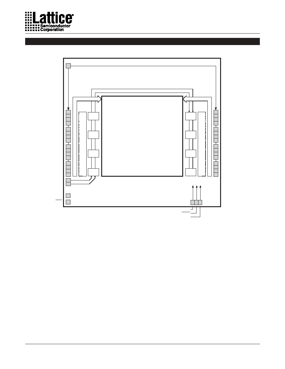
Functional Block Diagram
Figure 1. ispLSI 2032/A Functional Block Diagram
All of these signals are made available to the inputs of the
GLBs. Delays through the GRP have been equalized to
minimize timing skew.
Clocks in the ispLSI 2032 and 2032A devices are se-
lected using the dedicated clock pins. Three dedicated
clock pins (Y0, Y1, Y2) or an asynchronous clock can be
selected on a GLB basis. The asynchronous or Product
Term clock can be generated in any GLB for its own clock.
The devices also have 32 I/O cells, each of which is
directly connected to an I/O pin. Each I/O cell can be
individually programmed to be a combinatorial input,
output or bi-directional I/O pin with 3-state control. The
signal levels are TTL compatible voltages and the output
drivers can source 4 mA or sink 8 mA. Each output can
be programmed independently for fast or slow output
slew rate to minimize overall output switching noise.
Eight GLBs, 32 I/O cells, two dedicated inputs and two
ORPs are connected together to make a Megablock
(Figure 1). The outputs of the eight GLBs are connected
to a set of 32 universal I/O cells by the ORP. Each ispLSI
2032 and 2032A device contains one Megablock.
The GRP has as its inputs, the outputs from all of the
GLBs and all of the inputs from the bi-directional I/O cells.
Global Routing Pool
(GRP)
A0
A1
A3
Input
Bus
Output
Routing
Pool
(ORP)
A7
A6
A5
A4
Input
Bus
Output
Routing
Pool
(ORP)
A2
CLK
0
CLK
1
CLK
2
GOE 0
Notes:
*Y1 and RESET are multiplexed on the same pin
I/O 0
I/O 1
I/O 2
I/O 3
I/O 6
I/O 7
I/O 8
I/O 9
I/O 10
I/O 11
I/O 12
I/O 13
I/O 14
I/O 15
I/O 31
I/O 30
I/O 29
I/O 28
I/O 27
I/O 26
I/O 25
I/O 24
I/O 23
I/O 22
I/O 21
I/O 20
I/O 19
I/O 18
I/O 17
I/O 16
SDI/IN 0
SDO/IN 1
I/O 4
I/O 5
Y0
SCLK/Y2
ispEN
MODE
0139B(1)isp/2000
Y1*/RESET
Select
devices
have
been
discontinued.
See
Ordering
Information
section
for
product
status.
相關(guān)PDF資料 |
PDF描述 |
|---|---|
| EPM7128SQI100-10N | IC MAX 7000 CPLD 128 100-PQFP |
| RW2-0512S/H2/B | CONV DC/DC 2W 4.5-9VIN 12VOUT |
| MAX1792EUA25/V+T | IC REG LDO 2.5V/ADJ .5A 8-UMAX |
| M4A5-96/48-12VNI | IC CPLD 96MACRO 100TQFP |
| EPM7128SQI100-10 | IC MAX 7000 CPLD 128 100-PQFP |
相關(guān)代理商/技術(shù)參數(shù) |
參數(shù)描述 |
|---|---|
| ispLSI2032A-150LJN44 | 功能描述:CPLD - 復(fù)雜可編程邏輯器件 USE ispMACH 4000V RoHS:否 制造商:Lattice 系列: 存儲(chǔ)類(lèi)型:EEPROM 大電池?cái)?shù)量:128 最大工作頻率:333 MHz 延遲時(shí)間:2.7 ns 可編程輸入/輸出端數(shù)量:64 工作電源電壓:3.3 V 最大工作溫度:+ 90 C 最小工作溫度:0 C 封裝 / 箱體:TQFP-100 |
| ispLSI2032A-150LT44 | 功能描述:CPLD - 復(fù)雜可編程邏輯器件 USE ispMACH 4000V RoHS:否 制造商:Lattice 系列: 存儲(chǔ)類(lèi)型:EEPROM 大電池?cái)?shù)量:128 最大工作頻率:333 MHz 延遲時(shí)間:2.7 ns 可編程輸入/輸出端數(shù)量:64 工作電源電壓:3.3 V 最大工作溫度:+ 90 C 最小工作溫度:0 C 封裝 / 箱體:TQFP-100 |
| ISPLSI2032A-150LT44I | 制造商:LATTICE 制造商全稱(chēng):Lattice Semiconductor 功能描述:In-System Programmable High Density PLD |
| ispLSI2032A-150LT48 | 功能描述:CPLD - 復(fù)雜可編程邏輯器件 USE ispMACH 4000V RoHS:否 制造商:Lattice 系列: 存儲(chǔ)類(lèi)型:EEPROM 大電池?cái)?shù)量:128 最大工作頻率:333 MHz 延遲時(shí)間:2.7 ns 可編程輸入/輸出端數(shù)量:64 工作電源電壓:3.3 V 最大工作溫度:+ 90 C 最小工作溫度:0 C 封裝 / 箱體:TQFP-100 |
| ISPLSI2032A-150LT48I | 制造商:LATTICE 制造商全稱(chēng):Lattice Semiconductor 功能描述:In-System Programmable High Density PLD |
發(fā)布緊急采購(gòu),3分鐘左右您將得到回復(fù)。