- 您現(xiàn)在的位置:買賣IC網(wǎng) > PDF目錄384536 > ISPL1048E-125LQI (Lattice Semiconductor Corporation) High-Density Programmable Logic PDF資料下載
參數(shù)資料
| 型號: | ISPL1048E-125LQI |
| 廠商: | Lattice Semiconductor Corporation |
| 英文描述: | High-Density Programmable Logic |
| 中文描述: | 高密度可編程邏輯 |
| 文件頁數(shù): | 13/16頁 |
| 文件大小: | 158K |
| 代理商: | ISPL1048E-125LQI |
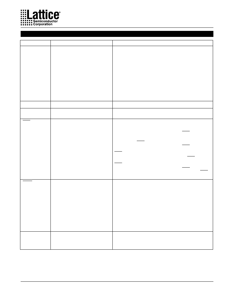
Specifications
ispLSI 1048E
13
1. NC pins are not to be connected to any active signals, VCC or GND.
Dedicated Clock input. This clock input is brought into the clock
distribution network, and can optionally be routed to any GLB on the
device.
Dedicated Clock input. This clock input is brought into the clock
distribution network, and can optionally be routed to any GLB and/or
any I/O cell on the device.
Dedicated Clock input. This clock input is brought into the clock
distribution network, and can optionally be routed to any I/O cell on the
device.
Dedicated Clock input. This clock input is connected to one of the clock
inputs of all of the GLBs on the device.
Input/Output Pins - These are the general purpose I/O pins used by the
logic array.
NAME
Table 2 - 0002C-48E
PQFP / TQFP PIN NUMBERS
DESCRIPTION
21,
27,
34,
40,
52,
58,
66,
72,
85,
91,
98,
104,
117,
123,
2,
8,
22,
28,
35,
41,
53,
59,
67,
73,
86,
92,
99,
105,
118,
124,
3,
9,
23,
29,
36,
42,
54,
60,
68,
74,
87,
93,
100,
106,
119,
125,
4,
10,
I/O 0 - I/O 5
I/O 6 - I/O 11
I/O 12 - I/O 17
I/O 18 - I/O 23
I/O 24 - I/O 29
I/O 30 - I/O 35
I/O 36 - I/O 41
I/O 42 - I/O 47
I/O 48 - I/O 53
I/O 54 - I/O 59
I/O 60 - I/O 65
I/O 66 - I/O 71
I/O 72 - I/O 77
I/O 78 - I/O 83
I/O 84 - I/O 89
I/O 90 - I/O 95
24,
30,
37,
43,
55,
61,
69,
75,
88,
94,
101,
107,
120,
126,
5,
11,
25,
31,
38,
44,
56,
62,
70,
76,
89,
95,
102,
108,
121,
127,
6,
12,
83
Y1
15
Y0
46
MODE/IN 1
Input - This pin performs two functions. When ispEN is logic low, it
functions as pin to control the operation of the isp state machine. When
ispEN is high, it functions as a dedicated input pin.
Output/Input - This pin performs two functions. When ispEN is logic low,
it functions as an output pin to read serial shift register data. When
ispEN is high, it functions as a dedicated input pin.
Input - This pin performs two functions. When ispEN is logic low, it
functions as a clock pin for the Serial Shift Register. When ispEN is
high, it functions as a dedicated input pin.
Ground (GND)
GND
V
VCC
CC
26,
32,
39,
45,
57,
63,
71,
77,
90,
96,
103,
109,
122,
128,
7,
13
Global Output Enable input pins.
GOE0, GOE1
Dedicated input pins to the device.
IN 2, IN 4
IN 6 - IN 11
64,
114
47,
84,
51
110,
111,
115,
116,
14
Input - Dedicated in-system programming enable input pin. This pin is
brought low to enable the programming mode. When low, the MODE,
SDI, SDO and SCLK controls become active.
Input - This pin performs two functions. When ispEN is logic low, it
functions as an input pin to load programming data into the device.
SDI/IN 0 also is used as one of the two control pins for the ISP state
machine. When ispEN is high, it functions as a dedicated input pin.
18
ispEN/NC
1
20
SDI/IN 0
50
SDO/IN 3
78
SCLK/IN 5
Active Low (0) Reset pin which resets all of the GLB and I/O registers in
the device.
19
RESET
80
Y2
79
Y3
1,
97,
16,
17,
112
48,
33,
49,
65,
81,
82,
113
Pin Description
相關(guān)PDF資料 |
PDF描述 |
|---|---|
| ISPL1048E-100LQ | High-Density Programmable Logic |
| ISPL1048E-100LQI | High-Density Programmable Logic |
| ISPL1048E-100LT | High-Density Programmable Logic |
| ISPL1048E-100LTI | High-Density Programmable Logic |
| ISPL1048E-125LQ | High-Density Programmable Logic |
相關(guān)代理商/技術(shù)參數(shù) |
參數(shù)描述 |
|---|---|
| ISPL1048E-125LT | 制造商:LATTICE 制造商全稱:Lattice Semiconductor 功能描述:High-Density Programmable Logic |
| ISPL1048E-125LTI | 制造商:LATTICE 制造商全稱:Lattice Semiconductor 功能描述:High-Density Programmable Logic |
| ISPL1048E-50LQ | 制造商:LATTICE 制造商全稱:Lattice Semiconductor 功能描述:High-Density Programmable Logic |
| ISPL1048E-50LQI | 制造商:LATTICE 制造商全稱:Lattice Semiconductor 功能描述:High-Density Programmable Logic |
| ISPL1048E-50LT | 制造商:LATTICE 制造商全稱:Lattice Semiconductor 功能描述:High-Density Programmable Logic |
發(fā)布緊急采購,3分鐘左右您將得到回復(fù)。