- 您現(xiàn)在的位置:買賣IC網(wǎng) > PDF目錄384535 > ISPGDX160VA-7B208 (LATTICE SEMICONDUCTOR CORP) In-System Programmable 3.3V Generic Digital CrosspointTM PDF資料下載
參數(shù)資料
| 型號(hào): | ISPGDX160VA-7B208 |
| 廠商: | LATTICE SEMICONDUCTOR CORP |
| 元件分類: | PLD |
| 英文描述: | In-System Programmable 3.3V Generic Digital CrosspointTM |
| 中文描述: | EE PLD, 7 ns, PBGA208 |
| 封裝: | FBGA-208 |
| 文件頁數(shù): | 3/37頁 |
| 文件大?。?/td> | 464K |
| 代理商: | ISPGDX160VA-7B208 |
第1頁第2頁當(dāng)前第3頁第4頁第5頁第6頁第7頁第8頁第9頁第10頁第11頁第12頁第13頁第14頁第15頁第16頁第17頁第18頁第19頁第20頁第21頁第22頁第23頁第24頁第25頁第26頁第27頁第28頁第29頁第30頁第31頁第32頁第33頁第34頁第35頁第36頁第37頁
3
Specifications
ispGDX160V/VA
Architecture
The ispGDXV/VA architecture is different from traditional
PLD architectures, in keeping with its unique application
focus. The block diagram is shown below. The program-
mable interconnect consists of a single Global Routing
Pool (GRP). Unlike ispLSI devices, there are no pro-
grammable logic arrays on the device. Control signals for
OEs, Clocks/Clock Enables and MUX Controls must
come from designated sets of I/O pins. The polarity of
these signals can be independently programmed in each
I/O cell.
Each I/O cell drives a unique pin. The OE control for each
I/O pin is independent and may be driven via the GRP by
one of the designated I/O pins (I/O-OE set). The I/O-OE
set consists of 25% of the total I/O pins. Boundary Scan
test is supported by dedicated registers at each I/O pin.
In-system programming is accomplished through the
standard Boundary Scan protocol.
The various I/O pin sets are also shown in the block
diagram below. The A, B, C, and D I/O pins are grouped
together with one group per side.
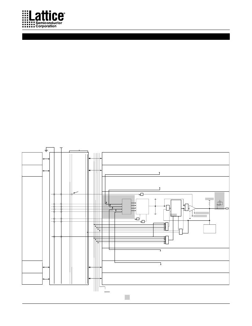
I/O Architecture
Each I/O cell contains a 4:1 dynamic MUX controlled by
two select lines as well as a 4x4 crossbar switch con-
trolled by software for increased routing flexiability (Figure
1). The four data inputs to the MUX (called M0, M1, M2,
and M3) come from I/O signals in the GRP and/or
adjacent I/O cells. Each MUX data input can access one
quarter of the total I/Os. For example, in a 160 I/O
ispGDXV, each data input can connect to one of 40 I/O
pins. MUX0 and MUX1 can be driven by designated I/O
pins called MUXsel1 and MUXsel2. Each MUXsel input
covers 25% of the total I/O pins (e.g. 40 out of 160). MUX0
and MUX1 can be driven from either MUXsel1 or MUXsel2.
Figure 1. ispGDXV/VA I/O Cell and GRP Detail (160 I/O Device)
I/OCell 0
I/O Cell 1
I/O Cell 78
I/O Cell 79
80 I/O Cells
Boundary
Bypass Option
I/O Cell N
or Latch
I/O
Pin
Prog.
(VCCIO)
Prog. Slew Rate
D
CLK
A
B
Reset
Q
4-to-1 MUX
M0
M1
M2
M3
MUX0
160 Input GRP
Outputs Horizontal
I/O Cell 159
I/O Cell 158
I/O Cell 81
I/O Group A
I/O Group B
I/O Group C
I/O Group D
4x4
Crossbar
Switch
MUX1
Global
Reset
I/O Cell 80
80 I/O Cells
ispGDXV/VA architecture enhancements over ispGDX (5V)
E
2
CMOS
Programmable
Interconnect
Logic
“
0
”
Logic
“
1
”
160 I/O Inputs
C
R
CloY0-Y3
Prog.
BLatch
CLK_EN
oFrom MUX Outputs
ofFrom MUX Outputs
To 2 Adjacent
I/O Cells above
ITo 2 Adjacent
Prog. Open Drain
2.5V/3.3V Output
N+1
N+2
N-1
N-2
相關(guān)PDF資料 |
PDF描述 |
|---|---|
| ISPGDX160VA-3B208 | In-System Programmable 3.3V Generic Digital CrosspointTM |
| ISPGDX160VA-3B272 | In-System Programmable 3.3V Generic Digital CrosspointTM |
| ISPGDX160VA-3Q208 | In-System Programmable 3.3V Generic Digital CrosspointTM |
| ISPGDX160VA-5B208 | In-System Programmable 3.3V Generic Digital CrosspointTM |
| ISPGDX160VA-5B208I | In-System Programmable 3.3V Generic Digital CrosspointTM |
相關(guān)代理商/技術(shù)參數(shù) |
參數(shù)描述 |
|---|---|
| ISPGDX160VA7B208-9I | 制造商:Lattice Semiconductor Corporation 功能描述: |
| ISPGDX160VA-7B208I | 功能描述:模擬和數(shù)字交叉點(diǎn) IC PROGRAMMABLE GEN DIG CROSSPOINT RoHS:否 制造商:Micrel 配置:2 x 2 封裝 / 箱體:MLF-16 數(shù)據(jù)速率:10.7 Gbps 輸入電平:CML, LVDS, LVPECL 輸出電平:CML 電源電壓-最大:3.6 V 電源電壓-最小:2.375 V 最大工作溫度:+ 85 C 最小工作溫度:- 40 C 產(chǎn)品:Digital Crosspoint 封裝:Tube |
| ISPGDX160VA-7B272 | 功能描述:模擬和數(shù)字交叉點(diǎn) IC PROGRAMMABLE GEN DIG CROSSPOINT RoHS:否 制造商:Micrel 配置:2 x 2 封裝 / 箱體:MLF-16 數(shù)據(jù)速率:10.7 Gbps 輸入電平:CML, LVDS, LVPECL 輸出電平:CML 電源電壓-最大:3.6 V 電源電壓-最小:2.375 V 最大工作溫度:+ 85 C 最小工作溫度:- 40 C 產(chǎn)品:Digital Crosspoint 封裝:Tube |
| ISPGDX160VA-7B272I | 功能描述:模擬和數(shù)字交叉點(diǎn) IC PROGRAMMABLE GEN DIG CROSSPOINT RoHS:否 制造商:Micrel 配置:2 x 2 封裝 / 箱體:MLF-16 數(shù)據(jù)速率:10.7 Gbps 輸入電平:CML, LVDS, LVPECL 輸出電平:CML 電源電壓-最大:3.6 V 電源電壓-最小:2.375 V 最大工作溫度:+ 85 C 最小工作溫度:- 40 C 產(chǎn)品:Digital Crosspoint 封裝:Tube |
| ISPGDX160VA-7BN208 | 功能描述:模擬和數(shù)字交叉點(diǎn) IC PROGRAMMABLE GEN DIG CROSSPOINT RoHS:否 制造商:Micrel 配置:2 x 2 封裝 / 箱體:MLF-16 數(shù)據(jù)速率:10.7 Gbps 輸入電平:CML, LVDS, LVPECL 輸出電平:CML 電源電壓-最大:3.6 V 電源電壓-最小:2.375 V 最大工作溫度:+ 85 C 最小工作溫度:- 40 C 產(chǎn)品:Digital Crosspoint 封裝:Tube |
發(fā)布緊急采購,3分鐘左右您將得到回復(fù)。