- 您現(xiàn)在的位置:買賣IC網(wǎng) > PDF目錄384532 > ISL9206DHZ-T (INTERSIL CORP) FlexiHash+ For Battery Authentication PDF資料下載
參數(shù)資料
| 型號: | ISL9206DHZ-T |
| 廠商: | INTERSIL CORP |
| 元件分類: | 電源管理 |
| 英文描述: | FlexiHash+ For Battery Authentication |
| 中文描述: | 1-CHANNEL POWER SUPPLY SUPPORT CKT, PDSO5 |
| 封裝: | 0.064 INCH, ROHS COMPLIANT, PLASTIC, EIAJ , SC-74, MO-178AA, SOT23, 5 PIN |
| 文件頁數(shù): | 13/17頁 |
| 文件大小: | 341K |
| 代理商: | ISL9206DHZ-T |
13
FN9260.2
January 5, 2007
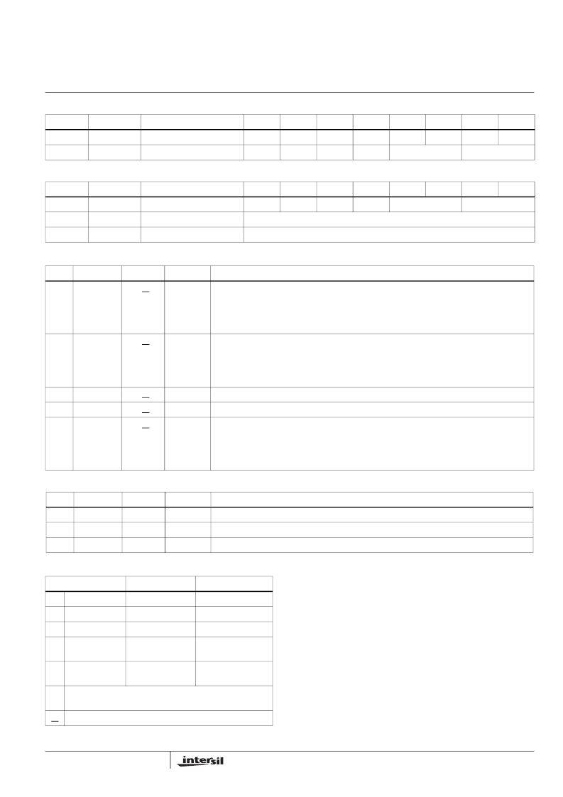
ADDRESS 0-00: DEFAULT CONFIGURATION (DCFG)
This address location stores the default configuration when
the ISL9206 is manufactured. Table 11 describes each bit in
detail. The legend for the TYPE column is given in Table 13.
ADDRESS 0-01: DEFAULT TRIM SETTING (DTRM)
This address location is writable only when the device is in
test mode. During normal operation, any data written to it will
be ignored. Table 12 describes the DTRM address in detail.
ADDRESS 0-02/03/04/05: AUTHENTICATION SECRET
SET #1 (SE1A/B/C/D)
These address locations store the first set of secrets to be
used for hash calculation. Reading and writing to this
register can be disabled by setting the SLO[1] bit at OTP
ROM location 0-00[1].
TABLE 9. CONTROL AND STATUS REGISTERS (BANK 1)
ADDRESS
NAME
DESCRIPTION
BIT 7
BIT 6
BIT 5
BIT 4
BIT3
BIT 2
BIT 1
BIT 0
1-00
MSCR
Master Control
eEEW
eINT
--
--
--
--
ASLP
SRST
1-01
STAT
Device Status
sEEW
sBER
sACC
--
DAB[1:0]
SLO[1:0]
TABLE 10. AUTHENTICATION REGISTERS (BANK 2)
ADDRESS
NAME
DESCRIPTION
BIT 7
BIT 6
BIT 5
BIT 4
BIT3
BIT 2
BIT 1
BIT 0
2-00
SESL
Secrets Selection
--
--
--
--
CSL[1:0]
SSL[1:0]
2-01
CHLG
Challenge Code Register
CHLG[31:0]
2-05
AUTH
Authentication Code Register
AUTH[7:0]
TABLE 11. DEFAULT CONFIGURATION (DCFG) REGISTER SETTINGS
BIT
NAME
TYPE
DEFAULT
DESCRIPTION
7:6
DAB[1:0]
RW
00
Device Address Bit Setting:
00 : device responds only when CS field in instruction frame is’0’
01 : device responds to any CS field value in instruction frame
10 : device responds to any CS field value in instruction frame
11 : device responds only when CS field in instruction frame is ‘1’
5:4
SPD[1:0]
RW
01
XSD Bus Speed Setting: Configures the bit rate of the XSD bus interface.
00 : 0.5x (2.89kbps)
01 : 1x (5.78kbps)
10 : 2x (11.56kbps)
11 : 4x (23.12kbps)
3
eINT
RW
1
Power-on default setting of eINT bit in the MSCR register.
2
ASLP
RW
1
Power-on default setting of ASLP bit in the MSCR register.
1:0
SLO[1:0]
RW
00
Secrets Lock-out Bits:
Bit 1 : Read/Write lock-out bit for address locations 0-02 to 0-09 (Secret Set #1 & #2)
Bit 0 : Read/Write lock-out bit for address locations 0-0A to 0-0D (Secret Set #3)
NOTE: Once Bit 0 or Bit 1 is set, writing to the OTP ROM will permanently be disabled
(after a reset cycle).
TABLE 12. DEFAULT TRIMMING (DTRM) REGISTER SETTINGS
BIT
NAME
TYPE
DEFAULT
DESCRIPTION
7
HSF
R
0
Unused
6:4
TIBB[2:0]
R
--
Reference Current Trim Setting
3:0
TOSC[3:0]
R
--
Oscillator Frequency Trim Setting
TABLE 13. LEGEND FOR THE TYPE COLUMN
TYPE
READ ACTION
WRITE ACTION
R
Read-only
Data read
Data ignored
W
Write-only
Zeros read
Data written
RW Read/Write
Data read
Data written
RC Clear after read
Data read, then
cleared
Data ignored
WC Clear after write
Zeros read
Data written, then
cleard
<>
Default setting loaded from designated OTP ROM bit
locations
W
Writing disabled after lock-out
ISL9206
相關(guān)PDF資料 |
PDF描述 |
|---|---|
| ISL9206 | FlexiHash+ For Battery Authentication |
| ISL9206_07 | FlexiHash+ For Battery Authentication |
| ISL9206DRZ-T | FlexiHash+ For Battery Authentication |
| ISL9206EVAL1 | FlexiHash For Battery Authentication |
| ISL9208IRZ | Multi-Cell Li-ion Battery Pack OCP/Analog Front End |
相關(guān)代理商/技術(shù)參數(shù) |
參數(shù)描述 |
|---|---|
| ISL9206DRZ | 制造商:Intersil Corporation 功能描述:IC SM CHARGER FLEXIHASH |
| ISL9206DRZ-T | 制造商:Intersil Corporation 功能描述:MULTI-CHEM 8TDFN - Tape and Reel 制造商:Intersil 功能描述:BATRY AUTHENTICATION DEVICE 2X3 |
| ISL9206EVAL1 | 制造商:Intersil Corporation 功能描述:EVAL BD FOR FLEXIHASH+ FOR BATTERY AUTHENTICATION - Bulk |
| ISL9208 | 制造商:INTERSIL 制造商全稱:Intersil Corporation 功能描述:Multi-Cell Li-ion Battery Pack OCP/Analog Front End |
| ISL9208_0711 | 制造商:INTERSIL 制造商全稱:Intersil Corporation 功能描述:Multi-Cell Li-ion Battery Pack OCP/Analog Front End |
發(fā)布緊急采購,3分鐘左右您將得到回復。