- 您現(xiàn)在的位置:買賣IC網(wǎng) > PDF目錄360968 > IRL531 TRANSISTOR | MOSFET | N-CHANNEL | 80V V(BR)DSS | 13A I(D) | TO-220AB PDF資料下載
參數(shù)資料
| 型號: | IRL531 |
| 英文描述: | TRANSISTOR | MOSFET | N-CHANNEL | 80V V(BR)DSS | 13A I(D) | TO-220AB |
| 中文描述: | 晶體管| MOSFET的| N溝道| 80V的五(巴西)直|第13A條(丁)| TO - 220AB現(xiàn)有 |
| 文件頁數(shù): | 2/10頁 |
| 文件大小: | 275K |
| 代理商: | IRL531 |
IRL530NS/L
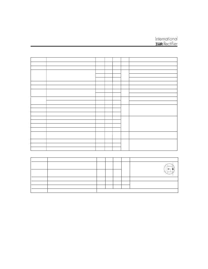
Parameter
Min. Typ. Max. Units
Conditions
MOSFET symbol
showing the
integral reverse
p-n junction diode.
T
J
= 25°C, I
S
= 9.0A, V
GS
= 0V
T
J
= 25°C, I
F
= 9.0A
di/dt = 100A/μs
I
S
Continuous Source Current
(Body Diode)
Pulsed Source Current
(Body Diode)
Diode Forward Voltage
Reverse Recovery Time
Reverse Recovery Charge
Forward Turn-On Time
–––
–––
I
SM
–––
–––
V
SD
t
rr
Q
rr
t
on
–––
–––
–––
Intrinsic turn-on time is negligible (turn-on is dominated by L
S
+L
D
)
–––
140
740 1100
1.3
210
V
ns
nC
Starting T
J
= 25°C, L = 3.1mH
R
G
= 25
, I
AS
= 9.0A. (See Figure 12)
I
SD
≤
9.0A, di/dt
≤
540A/μs, V
DD
≤
V
(BR)DSS
,
T
J
≤
175°C
Repetitive rating; pulse width limited by
max. junction temperature. ( See fig. 11 )
Notes:
Pulse width
≤
300μs; duty cycle
≤
2%.
Uses IRL530N data and test conditions
** When mounted on 1" square PCB ( FR-4 or G-10 Material ).
For recommended soldering techniques refer to application note #AN-994.
Source-Drain Ratings and Characteristics
S
D
G
17
60
A
Parameter
Min. Typ. Max. Units
100
–––
–––
0.122 –––
–––
––– 0.100
–––
––– 0.120
–––
––– 0.150
1.0
–––
7.7
–––
–––
–––
–––
–––
–––
–––
–––
–––
–––
–––
–––
–––
–––
–––
–––
7.2
–––
53
–––
30
–––
26
Conditions
V
GS
= 0V, I
D
= 250μA
Reference to 25°C, I
D
= 1mA
V
GS
= 10V, I
D
= 9.0A
V
GS
= 5.0V, I
D
= 9.0A
V
GS
= 4.0V, I
D
= 8.0A
V
DS
= V
GS
, I
D
= 250μA
V
DS
= 50V, I
D
= 9.0A
V
DS
= 100V, V
GS
= 0V
V
DS
= 80V, V
GS
= 0V, T
J
= 150°C
V
GS
= 16V
V
GS
= -16V
I
D
= 9.0A
V
DS
= 80V
V
GS
= 5.0V, See Fig. 6 and 13
V
DD
= 50V
I
D
= 9.0A
R
G
= 6.0
,
V
GS
= 5.0V
R
D
= 5.5
,
See Fig. 10
Between lead,
and center of die contact
V
GS
= 0V
V
DS
= 25V
= 1.0MHz, See Fig. 5
V
(BR)DSS
V
(BR)DSS
/
T
J
Breakdown Voltage Temp. Coefficient
Drain-to-Source Breakdown Voltage
–––
V
V/°C
V
GS(th)
g
fs
Gate Threshold Voltage
Forward Transconductance
2.0
–––
25
250
100
-100
34
4.8
20
–––
–––
–––
–––
V
S
Gate-to-Source Forward Leakage
Gate-to-Source Reverse Leakage
Total Gate Charge
Gate-to-Source Charge
Gate-to-Drain ("Miller") Charge
Turn-On Delay Time
Rise Time
Turn-Off Delay Time
Fall Time
nA
Q
g
Q
gs
Q
gd
t
d(on)
t
r
t
d(off)
t
f
nC
–––
–––
C
iss
C
oss
C
rss
Input Capacitance
Output Capacitance
Reverse Transfer Capacitance
–––
–––
–––
800
160
90
–––
–––
–––
pF
Electrical Characteristics @ T
J
= 25°C (unless otherwise specified)
I
GSS
I
DSS
Drain-to-Source Leakage Current
R
DS(on)
Static Drain-to-Source On-Resistance
L
S
Internal Source Inductance
7.5
ns
nH
A
相關(guān)PDF資料 |
PDF描述 |
|---|---|
| IRL540 | (166.75 k) |
| IRL541 | TRANSISTOR | MOSFET | N-CHANNEL | 80V V(BR)DSS | 24A I(D) | TO-220AB |
| IRL5602STRL | TRANSISTOR | MOSFET | P-CHANNEL | 20V V(BR)DSS | 24A I(D) | TO-263AB |
| IRL5602STRR | TRANSISTOR | MOSFET | P-CHANNEL | 20V V(BR)DSS | 24A I(D) | TO-263AB |
| IRL5NJ7413 | 30V Single N-Channel Hi-Rel MOSFET in a SMD-0.5 package |
相關(guān)代理商/技術(shù)參數(shù) |
參數(shù)描述 |
|---|---|
| IRL540 | 功能描述:MOSFET N-Chan 100V 28 Amp RoHS:否 制造商:STMicroelectronics 晶體管極性:N-Channel 汲極/源極擊穿電壓:650 V 閘/源擊穿電壓:25 V 漏極連續(xù)電流:130 A 電阻汲極/源極 RDS(導(dǎo)通):0.014 Ohms 配置:Single 最大工作溫度: 安裝風(fēng)格:Through Hole 封裝 / 箱體:Max247 封裝:Tube |
| IRL540A | 功能描述:MOSFET 100V N-Channel a-FET Logic Level RoHS:否 制造商:STMicroelectronics 晶體管極性:N-Channel 汲極/源極擊穿電壓:650 V 閘/源擊穿電壓:25 V 漏極連續(xù)電流:130 A 電阻汲極/源極 RDS(導(dǎo)通):0.014 Ohms 配置:Single 最大工作溫度: 安裝風(fēng)格:Through Hole 封裝 / 箱體:Max247 封裝:Tube |
| IRL540L | 功能描述:MOSFET N-Chan 100V 28 Amp RoHS:否 制造商:STMicroelectronics 晶體管極性:N-Channel 汲極/源極擊穿電壓:650 V 閘/源擊穿電壓:25 V 漏極連續(xù)電流:130 A 電阻汲極/源極 RDS(導(dǎo)通):0.014 Ohms 配置:Single 最大工作溫度: 安裝風(fēng)格:Through Hole 封裝 / 箱體:Max247 封裝:Tube |
| IRL540N | 制造商:International Rectifier 功能描述:MOSFET N LOGIC TO-220 |
| IRL540NHR | 制造商:International Rectifier 功能描述:Trans MOSFET N-CH 100V 36A 3-Pin(3+Tab) TO-220AB 制造商:International Rectifier 功能描述:TRANS MOSFET N-CH 100V 36A 3PIN TO-220AB - Rail/Tube |
發(fā)布緊急采購,3分鐘左右您將得到回復(fù)。