- 您現(xiàn)在的位置:買賣IC網(wǎng) > PDF目錄384503 > IRHM7450 (International Rectifier) REPETITIVE AVALANCHE AND dv/dt RATED PDF資料下載
參數(shù)資料
| 型號: | IRHM7450 |
| 廠商: | International Rectifier |
| 英文描述: | REPETITIVE AVALANCHE AND dv/dt RATED |
| 中文描述: | 重復(fù)性雪崩和dv / dt受好評 |
| 文件頁數(shù): | 3/12頁 |
| 文件大小: | 311K |
| 代理商: | IRHM7450 |
IRHM7450, IRHM8450, JANSR-, JANSH-, 2N7270 Devices
www.irf.com
3
Radiation Performance of Rad Hard HEXFETs
International Rectifier Radiation Hardened HEXFETs
are tested to verify their hardness capability. The hard-
ness assurance program at International Rectifier
comprises three radiation environments.
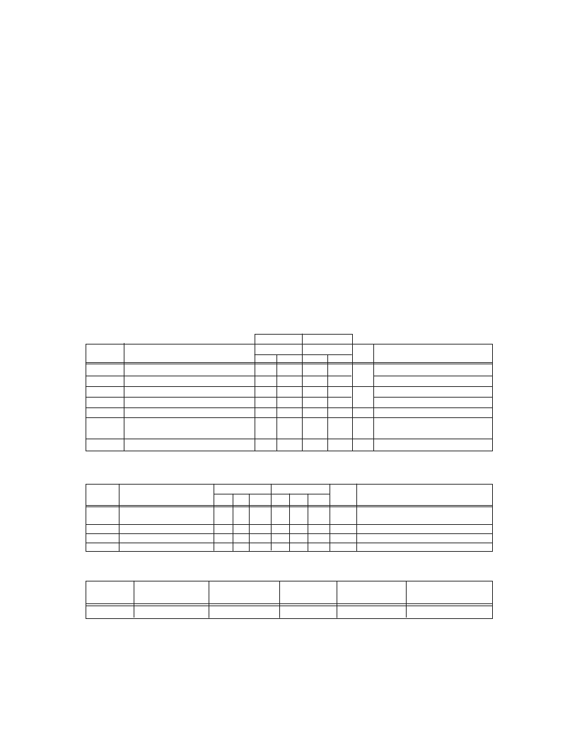
Table 1. Low Dose Rate
Parameter
IRHM7450 IRHM8450
100K Rads (Si) 1000K Rads (Si)
Units
Min
Max
Min
500
—
500
2.0
4.0
1.25
—
100
—
—
-100
—
—
50
—
—
0.45
—
Test Conditions
Max
—
4.5
100
-100
50
0.6
BV
DSS
V
GS(th)
I
GSS
I
GSS
I
DSS
R
DS(on)1
Drain-to-Source Breakdown Voltage
Gate Threshold Voltage
Gate-to-Source Leakage Forward
Gate-to-Source Leakage Reverse
Zero Gate Voltage Drain Current
Static Drain-to-Source
On-State Resistance One
Diode Forward Voltage
V
V
GS
= 0V, I
D
= 1.0mA
V
GS
= V
DS
, I
D
= 1.0mA
V
GS
= 20V
V
GS
= -20 V
V
DS
=0.8 x Max Rating, V
GS
=0V
V
GS
= 12V, I
D
= 7.0A
nA
μA
V
SD
—
1.6
—
1.6
V
TC = 25°C, IS =11A,V
GS
= 0V
Every manufacturing lot is tested in a low dose rate
(total dose) environment per MIL-STD-750, test
method 1019 condition A. International Rectifier has
imposed a standard gate condition of 12 volts per
note 6 and a V
bias condition equal to 80% of the
device rated voltage per note 7. Pre- and post- irra-
diation limits of the devices irradiated to 1 x 10
5
Rads
(Si) are identical and are presented in Table 1, col-
umn 1, IRHM7450. Post-irradiation limits of the de-
vices irradiated to 1 x 10
6
Rads (Si) are presented in
Table 1, column 2, IRHM8450. The values in Table 1
will be met for either of the two low dose rate test
circuits that are used. Both pre- and post-irradiation
performance are tested and specified using the same
drive circuitry and test conditions in order to provide a
direct comparison.
High dose rate testing may be done on a special
request basis using a dose rate up to 1 x 10
12
Rads
(Si)/Sec (See Table 2).
International Rectifier radiation hardened HEXFETs
have been characterized in heavy ion Single Event
Effects (SEE) environments. Single Event Effects char-
acterization is shown in Table 3.
Table 2. High Dose Rate
10
11
Rads (Si)/sec 10
12
Rads (Si)/sec
Min Typ Max
—
—
400
Parameter
Drain-to-Source Voltage
Min Typ Max
Units
—
—
400
Test Conditions
V
DSS
V
Applied drain-to-source voltage during
gamma-dot
Peak radiation induced photo-current
A/μsec Rate of rise of photo-current
μH
Circuit inductance required to limit di/dt
IPP
di/dt
L1
—
—
27
8
—
—
—
15
—
—
—
133
8
—
—
—
3
—
A
Table 3. Single Event Effects
LET (Si)
Fluence Range V
DS
Bias V
GS
Bias
Ion
(MeV/mg/cm
2
) (ions/cm
2
) (μm) (V) (V)
Ni 28
3x 10
5
~41 275 -5
Radiation
Characteristics
相關(guān)PDF資料 |
PDF描述 |
|---|---|
| IRHM7450SE | TRANSISTOR N-CHANNEL(BVdss=500V, Rds(on)=0.51ohm, Id=12A) |
| IRHM8450 | REPETITIVE AVALANCHE AND dv/dt RATED |
| IRHM9064 | TRANSISTOR P-CHANNEL(BVdss=-60V, Rds(on)=0.060ohm, Id=-35*A) |
| IRHM9150 | RADIATION HARDENED POWER MOSFET THRU-HOLE (TO-254AA) |
| IRHM93150 | RADIATION HARDENED POWER MOSFET THRU-HOLE (TO-254AA) |
相關(guān)代理商/技術(shù)參數(shù) |
參數(shù)描述 |
|---|---|
| IRHM7450_06 | 制造商:IRF 制造商全稱:International Rectifier 功能描述:RADIATION HARDENED POWER MOSFET THRU-HOLE (TO-254AA) |
| IRHM7450D | 制造商:未知廠家 制造商全稱:未知廠家 功能描述:TRANSISTOR | MOSFET | N-CHANNEL | 500V V(BR)DSS | 11A I(D) | TO-254VAR |
| IRHM7450SCS | 制造商:International Rectifier 功能描述:HIREL, HEXFET RHD - Bulk |
| IRHM7450SE | 制造商:IRF 制造商全稱:International Rectifier 功能描述:TRANSISTOR N-CHANNEL(BVdss=500V, Rds(on)=0.51ohm, Id=12A) |
| IRHM7450SESCS | 制造商:International Rectifier 功能描述:HIREL, HEXFET RHD - Bulk |
發(fā)布緊急采購,3分鐘左右您將得到回復(fù)。