- 您現(xiàn)在的位置:買賣IC網(wǎng) > PDF目錄384488 > IRF1312PBF (International Rectifier) HEXFET Power MOSFET PDF資料下載
參數(shù)資料
| 型號: | IRF1312PBF |
| 廠商: | International Rectifier |
| 英文描述: | HEXFET Power MOSFET |
| 中文描述: | HEXFET功率MOSFET |
| 文件頁數(shù): | 2/11頁 |
| 文件大?。?/td> | 286K |
| 代理商: | IRF1312PBF |
2
www.irf.com
Parameter
Min. Typ. Max. Units
92
–––
–––
93 140 I
D
= 57A
–––
36
–––
–––
34
–––
–––
25
–––
–––
130
–––
–––
47
–––
–––
51
–––
–––
5450
–––
–––
550
–––
–––
340
–––
–––
1910
–––
–––
380
–––
–––
620
–––
Conditions
V
DS
= 25V, I
D
= 57A
g
fs
Q
g
Q
gs
Q
gd
t
d(on)
t
r
t
d(off)
t
f
C
iss
C
oss
C
rss
C
oss
C
oss
C
oss
eff.
Forward Transconductance
Total Gate Charge
Gate-to-Source Charge
Gate-to-Drain ("Miller") Charge
Turn-On Delay Time
Rise Time
Turn-Off Delay Time
Fall Time
Input Capacitance
Output Capacitance
Reverse Transfer Capacitance
Output Capacitance
Output Capacitance
Effective Output Capacitance
–––
S
nC
V
DS
= 40V
V
GS
= 10V,
V
DD
= 40V
I
D
= 57A
R
G
= 4.5
V
GS
= 10V
V
GS
= 0V
V
DS
= 25V
= 1.0MHz
V
GS
= 0V, V
DS
= 1.0V, = 1.0MHz
V
GS
= 0V, V
DS
= 64V, = 1.0MHz
V
GS
= 0V, V
DS
= 0V to 64V
pF
Dynamic @ T
J
= 25°C (unless otherwise specified)
ns
Parameter
Typ.
–––
–––
–––
Max.
250
57
21
Units
mJ
A
mJ
E
AS
I
AR
E
AR
Single Pulse Avalanche Energy
Avalanche Current
Repetitive Avalanche Energy
Avalanche Characteristics
S
D
G
Parameter
Min. Typ. Max. Units
Conditions
I
S
Continuous Source Current
(Body Diode)
Pulsed Source Current
(Body Diode)
Diode Forward Voltage
Reverse Recovery Time
Reverse RecoveryCharge
Forward Turn-On Time
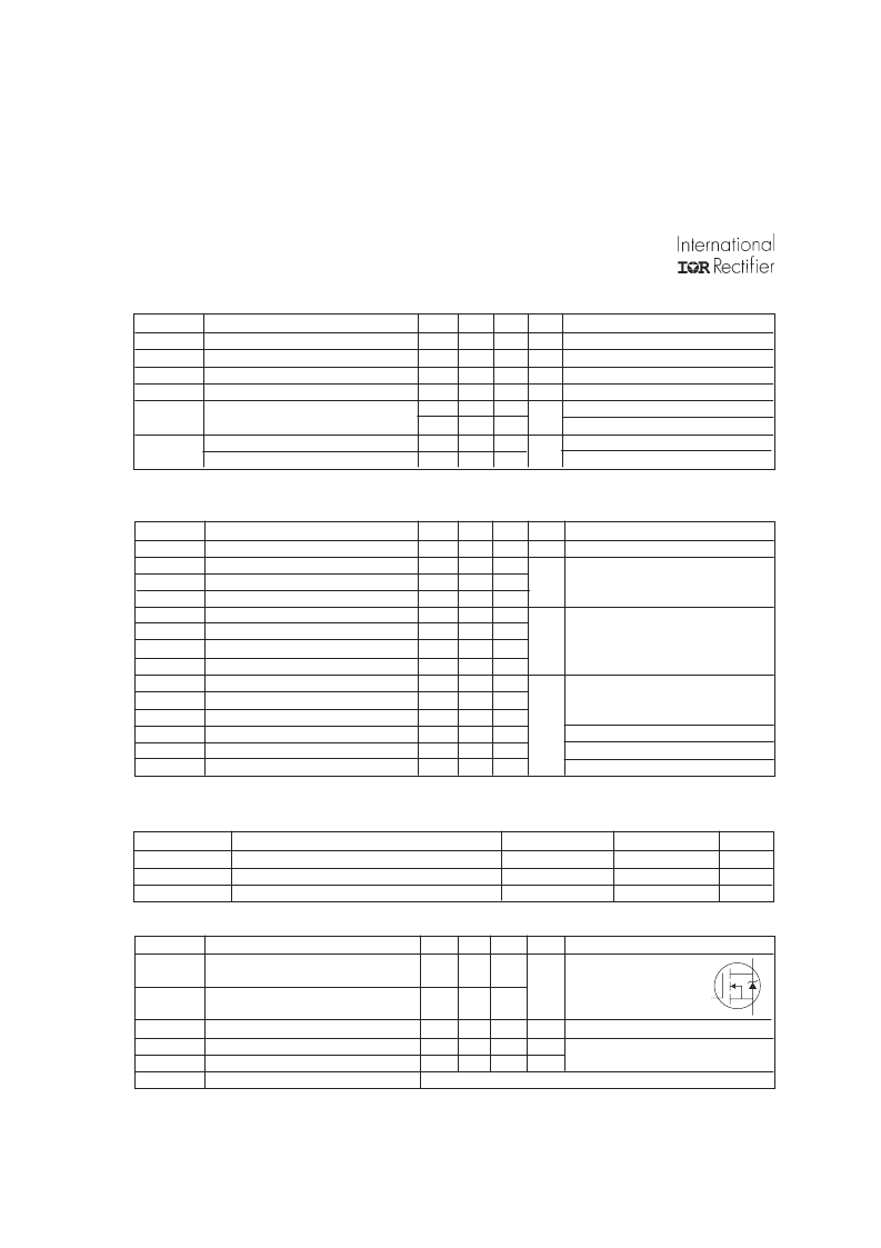
MOSFET symbol
showing the
integral reverse
p-n junction diode.
T
J
= 25°C, I
S
= 57A, V
GS
= 0V
T
J
= 25°C, I
F
= 57A
di/dt = 100A/μs
–––
–––
I
SM
–––
–––
V
SD
t
rr
Q
rr
t
on
–––
–––
–––
–––
64
150
1.3
96
230
V
ns
nC
Intrinsic turn-on time is negligible (turn-on is dominated by L
S
+L
D
)
Diode Characteristics
95
380
Static @ T
J
= 25°C (unless otherwise specified)
Parameter
V
(BR)DSS
Drain-to-Source Breakdown Voltage
V
(BR)DSS
/
T
J
Breakdown Voltage Temp. Coefficient
––– 0.078 ––– V/°C Reference to 25°C, I
D
= 1mA
R
DS(on)
Static Drain-to-Source On-Resistance
–––
V
GS(th)
Gate Threshold Voltage
3.5
–––
–––
Gate-to-Source Forward Leakage
–––
Gate-to-Source Reverse Leakage
–––
Min. Typ. Max. Units
80
–––
Conditions
V
GS
= 0V, I
D
= 250μA
–––
V
6.6
–––
–––
–––
–––
–––
10
5.5
1.0
250
100
-100
m
V
V
GS
= 10V, I
D
= 57A
V
DS
= V
GS
, I
D
= 250μA
V
DS
= 76V, V
GS
= 0V
V
DS
= 64V, V
GS
= 0V, T
J
= 150°C
V
GS
= 20V
V
GS
= -20V
μA
nA
I
GSS
I
DSS
Drain-to-Source Leakage Current
相關(guān)PDF資料 |
PDF描述 |
|---|---|
| IRF1312SPbF | HEXFET Power MOSFET |
| IRF1503SPBF | HEXFET Power MOSFET |
| IRF1704 | Power MOSFET(Vdss=40V, Rds(on)=0.004ohm, Id=170A) |
| IRF1730G | Power MOSFET(Vdss=400V, Rds(on)=1.0ohm, Id=3.7A) |
| IRFI730G | HEXFET POWER MOSFET |
相關(guān)代理商/技術(shù)參數(shù) |
參數(shù)描述 |
|---|---|
| IRF1312S | 制造商:IRF 制造商全稱:International Rectifier 功能描述:HEXFET Power MOSFET |
| IRF1312SHR | 制造商:International Rectifier 功能描述:Trans MOSFET N-CH 80V 95A 3-Pin(2+Tab) D2PAK 制造商:International Rectifier 功能描述:TRANS MOSFET N-CH 80V 95A 3PIN D2PAK - Rail/Tube |
| IRF1312SPBF | 制造商:IRF 制造商全稱:International Rectifier 功能描述:HEXFET Power MOSFET |
| IRF1312STRL | 制造商:International Rectifier 功能描述: |
| IRF1312STRR | 制造商:IRF 制造商全稱:International Rectifier 功能描述:TRANSISTOR | MOSFET | N-CHANNEL | 80V V(BR)DSS | 95A I(D) | TO-263AB |
發(fā)布緊急采購,3分鐘左右您將得到回復(fù)。