- 您現(xiàn)在的位置:買賣IC網(wǎng) > Datasheet目錄40 > IR22771STRPBF (International Rectifier)IC CURRENT SENSE 16SOIC Datasheet資料下載
參數(shù)資料
| 型號(hào): | IR22771STRPBF |
| 廠商: | International Rectifier |
| 文件頁(yè)數(shù): | 9/16頁(yè) |
| 文件大?。?/td> | 441K |
| 描述: | IC CURRENT SENSE 16SOIC |
| 標(biāo)準(zhǔn)包裝: | 500 |
| 功能: | 電流感應(yīng) |
| 輸入電壓: | 8 V ~ 20 V |
| 工作溫度: | -40°C ~ 125°C |
| 安裝類型: | 表面貼裝 |
| 封裝/外殼: | 16-SOIC(0.295",7.50mm 寬) |
| 供應(yīng)商設(shè)備封裝: | 16-SOIC |
| 包裝: | 帶卷 (TR) |
第1頁(yè)第2頁(yè)第3頁(yè)第4頁(yè)第5頁(yè)第6頁(yè)第7頁(yè)第8頁(yè)當(dāng)前第9頁(yè)第10頁(yè)第11頁(yè)第12頁(yè)第13頁(yè)第14頁(yè)第15頁(yè)第16頁(yè)
IR22771S/IR21771S(PbF)
9
www.irf.com
1 DEVICE DESCRIPTION
1.1 SYNC input
Sync input clocks the whole device. In order to
make the device work properly it must be
synchronous with the triangular PWM carrier as
shown in Figure 8.
SYNC pin is internally pulled-down (10 k&) to V
SS
.
1.2 PWM Output (PO)
PWM output is an open collector output (active low).
It must be pulled-up to proper supply with an
external resistor (suggested value between 500&
and 10k&).
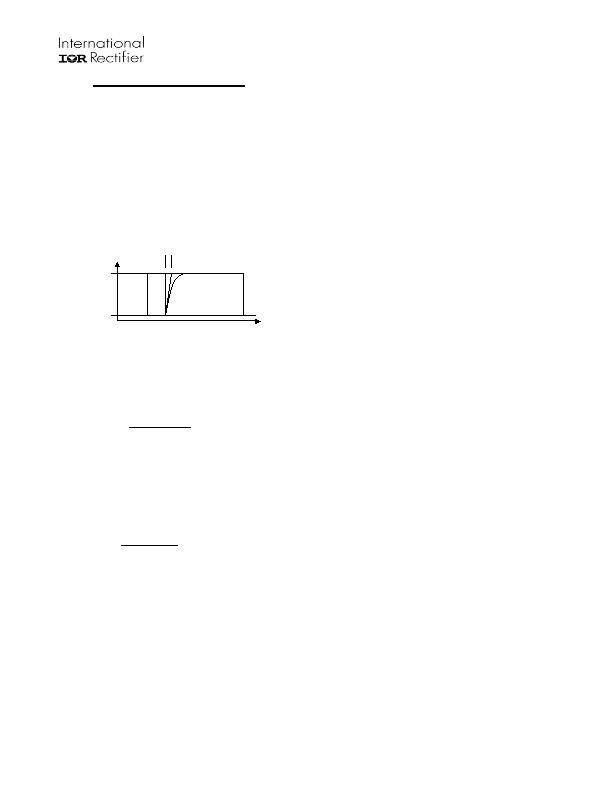
Figure 7: PO rising and falling slopes
PO pull-up resistor determines the rising slope of
the PO output and the lower value of PO as shown
in Figure 7, where RC
= , C is the total PO pin
capacitance and R is the pull-up resistance.
up
pull
on
on
low
R
R
R
Supply
V
+
?/DIV>
=
where R
on
is the internal open collector resistance
and R
pull-up
is the external pull-up resistance.
PO duty cycle is defined for active low logic by the
following formula:
Eq. 1
n
cycle
n
cycle
off
n
T
T
D
_
1
_
_
+
=
PO duty cycle (D
n
) swings between 10% and 30%.
Zero input voltage corresponds to 20% duty cycle.
A residual offset can be read in PO duty cycle
according to V
POs
(see Static electrical
characteristics).
According to Figure 8, it can be assumed that odd
cycles are represented by SYNC at high level
(channel 1) and even cycles represented by SYNC
at low level (channel 2).
The two channels are independent in order to
provide the correct duty cycle value of PO even for
non-50% duty cycle of SYNC signal. Small variation
of SYNC duty cycle are then allowed and
automatically corrected when calculating the duty
cycle using Eq. 1.
However, channel 1 and channel 2 can have a
difference in offset value which is specified in
V
POS
(see Static electrical characteristics).
To implement a correct offset compensation of PO
duty cycle, each channel must be compensated
separately.
1.3 Over Current output (OC)
OC output is an open drain pin (active low).
A simplified block diagram of the over current circuit
is shown in the Figure 9.
Over current is detected when |V
in
|=|V
inp
-V
inm
|>V
OCth
.
If an event of over current lasts longer than t
dOCon
,
OC pin is forced to V
SS
and remains latched until
PO is externally forced low for at least t
OCoff
(see
timing on Figure 4). During an over current event
(OC is low), PO is off (pulled-up by external
resistor).
If OC is reset by PO and over current is still active,
OC pin will be forced low again by the next edge of
SYNC signal.
To reset OC state PO must be forced to V
SS
for at
least T
OCoff
.
" Auto reset function
The auto reset function consists in clearing
automatically the OC fault.
To enable the auto reset function, simply short
circuit the OC pin with the PO pin.
?
V
low
Supply
相關(guān)PDF資料 |
PDF描述 |
|---|---|
| IRU3073CQTR | IC REG DL BCK/LINEAR 16-QSOP |
| ISL25700FRUZ-TK | IC TEMP SWITCH MFET DRVR 10TQFN |
| ISL6150IB | IC CTRLR HOT PLUG NEG VOLT 8SOIC |
| ISL6151IB-T | IC CTRLR HOT PLUG NEG VOLT 8SOIC |
| ISL6160CB-T | IC CTRLR BULK/AUXILIARY 14-SOIC |
相關(guān)代理商/技術(shù)參數(shù) |
參數(shù)描述 |
|---|---|
| IR2277S | 制造商:IRF 制造商全稱:International Rectifier 功能描述:Phase Current Sensor IC for AC motor control |
| IR2277SPBF | 功能描述:馬達(dá)/運(yùn)動(dòng)/點(diǎn)火控制器和驅(qū)動(dòng)器 1200V PHASE CURRENT SENSING IC RoHS:否 制造商:STMicroelectronics 產(chǎn)品:Stepper Motor Controllers / Drivers 類型:2 Phase Stepper Motor Driver 工作電源電壓:8 V to 45 V 電源電流:0.5 mA 工作溫度:- 25 C to + 125 C 安裝風(fēng)格:SMD/SMT 封裝 / 箱體:HTSSOP-28 封裝:Tube |
| IR2277STRPBF | 功能描述:馬達(dá)/運(yùn)動(dòng)/點(diǎn)火控制器和驅(qū)動(dòng)器 1200VPhs Cur Sens IC for AC Mtr Cntrl RoHS:否 制造商:STMicroelectronics 產(chǎn)品:Stepper Motor Controllers / Drivers 類型:2 Phase Stepper Motor Driver 工作電源電壓:8 V to 45 V 電源電流:0.5 mA 工作溫度:- 25 C to + 125 C 安裝風(fēng)格:SMD/SMT 封裝 / 箱體:HTSSOP-28 封裝:Tube |
| IR22GJ | 制造商:SGX Sensortech 功能描述:Series 2 Hydrocarbon IR Sensor with temp. sens IC ( IS for mining), Bulk |
| IR-2-3.3-10 | 制造商:Vishay Dale 功能描述:Inductor, Iron Core, 3.3uh, 10±% |
發(fā)布緊急采購(gòu),3分鐘左右您將得到回復(fù)。