- 您現(xiàn)在的位置:買賣IC網(wǎng) > PDF目錄360851 > IMIZ9952 Clocks and Buffers PDF資料下載
參數(shù)資料
| 型號: | IMIZ9952 |
| 英文描述: | Clocks and Buffers |
| 中文描述: | 時鐘和緩沖器 |
| 文件頁數(shù): | 3/9頁 |
| 文件大?。?/td> | 50K |
| 代理商: | IMIZ9952 |
3.3V, 180MHz, Multi-Output Zero Delay Buffer
Cypress Semiconductor Corporation
http://www.cypress.com
Document#: 38-07084 Rev. *B
12/22/2002
Page 3 of 9
Z9951
Maximum Ratings1
Maximum Input Voltage Relative to VSS: VSS - 0.3V
Maximum Input Voltage Relative to VDD: VDD + 0.3V
Storage Temperature:
Operating Temperature:
Maximum ESD protection
Maximum Power Supply:
Maximum Input Current:
-65
°
C to + 150
°
C
-40
°
C to +85
°
C
2KV
5.5V
±
20mA
This device contains circuitry to protect the inputs
against damage due to high static voltages or electric
field; however, precautions should be taken to avoid
application of any voltage higher than the maximum
rated voltages to this circuit. For proper operation, Vin
and Vout should be constrained to the range:
VSS<(Vin or Vout)<VDD
Unused inputs must always be tied to an appropriate
logic voltage level (either VSS or VDD).
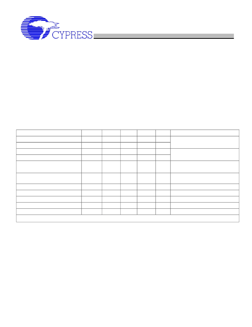
DC Parameters
Characteristic
Input Low Voltage
Input High Voltage
Input Low Current (@VIL = VSS)
Input High Current (@VIL =VDD)
Peak-to-Peak Input Voltage
PECL_CLK
Common Mode Range
PECL_CLK
Output Low Voltage
Output High Voltage
Quiescent Supply Current
PLL Supply Current
Input Capacitance
Symbol
VIL
VIH
IIL
IIH
VPP
Min
VSS
2.0
Typ
Max
Units
V
V
μA
μA
mV
Conditions
-
-
0.8
VDD
-120
120
1000
Note 2
300
Note 3
VCMR
VDD-
2.0
-
VDD-
0.6
0.5
V
VOL
VOH
IDDC
IDD
Cin
V
V
IOL = 40mA, Note 4
IOH = -40mA, Note 4
All VDDC and VDD
VDD only
2.4
-
-
-
15
15
-
20
20
4
mA
mA
pF
VDD = VDDC = 3.3V
±
5%, TA = -40
°
C to +85
°
C
Note 1:
The voltage on any input or I/O pin cannot exceed the power pin during power-up. Power supply sequencing is NOT
required.
Note 2:
Inputs have pull-up, pull-down resistors that affect input current.
Note 3:
The VCMR is the difference from the most positive side of the differential input signal. Normal operation is obtained when
the “High” input is within the VCMR range and the input lies within the VPP specification.
Note 4:
Driving series or parallel terminated 50
(or 50
to VDD/2) transmission lines. Output buffers are dual staged to control
drive strength in order to reduce over / under shoot.
相關(guān)PDF資料 |
PDF描述 |
|---|---|
| IMIZ9960 | Clocks and Buffers |
| IMIZ9973 | Clocks and Buffers |
| IMIZ9974 | Clocks and Buffers |
| IMIZ9975 | Clocks and Buffers |
| IMIZ9104DAB | SIX DISTRIBUTED-OUTPUT CLOCK DRIVER|TQFP|32PIN|PLASTIC |
相關(guān)代理商/技術(shù)參數(shù) |
參數(shù)描述 |
|---|---|
| IMIZ9952AA | 制造商:Rochester Electronics LLC 功能描述:ZERO DELAY BUFFER. 11 OUTPUTS, 180MHZ, 3.3V - Bulk 制造商:Cypress Semiconductor 功能描述: |
| IMIZ9952AAT | 制造商:Rochester Electronics LLC 功能描述:ZERO DELAY BUFFER. 11 OUTPUTS, 180MHZ, 3.3V T/R - Bulk 制造商:Cypress Semiconductor 功能描述: |
| IMIZ9953AA | 制造商:Rochester Electronics LLC 功能描述:ZERO DELAY BUFFER. 8 OUTPUTS, 110MHZ, 3.3V - Bulk |
| IMIZ9960 | 制造商:未知廠家 制造商全稱:未知廠家 功能描述:Clocks and Buffers |
| IMIZ9960AL | 制造商:CYPRESS 制造商全稱:Cypress Semiconductor 功能描述:2.5V/3.3V, 200 MHz Multi-Output Zero Delay Buffer |
發(fā)布緊急采購,3分鐘左右您將得到回復(fù)。