- 您現(xiàn)在的位置:買賣IC網 > PDF目錄65589 > IDT74FST163210PA8 (INTEGRATED DEVICE TECHNOLOGY INC) CBT/FST/QS/5C/B SERIES, DUAL 10-BIT DRIVER, TRUE OUTPUT, PDSO48 PDF資料下載
參數(shù)資料
| 型號: | IDT74FST163210PA8 |
| 廠商: | INTEGRATED DEVICE TECHNOLOGY INC |
| 元件分類: | 總線收發(fā)器 |
| 英文描述: | CBT/FST/QS/5C/B SERIES, DUAL 10-BIT DRIVER, TRUE OUTPUT, PDSO48 |
| 封裝: | TSSOP-48 |
| 文件頁數(shù): | 4/6頁 |
| 文件大?。?/td> | 68K |
| 代理商: | IDT74FST163210PA8 |
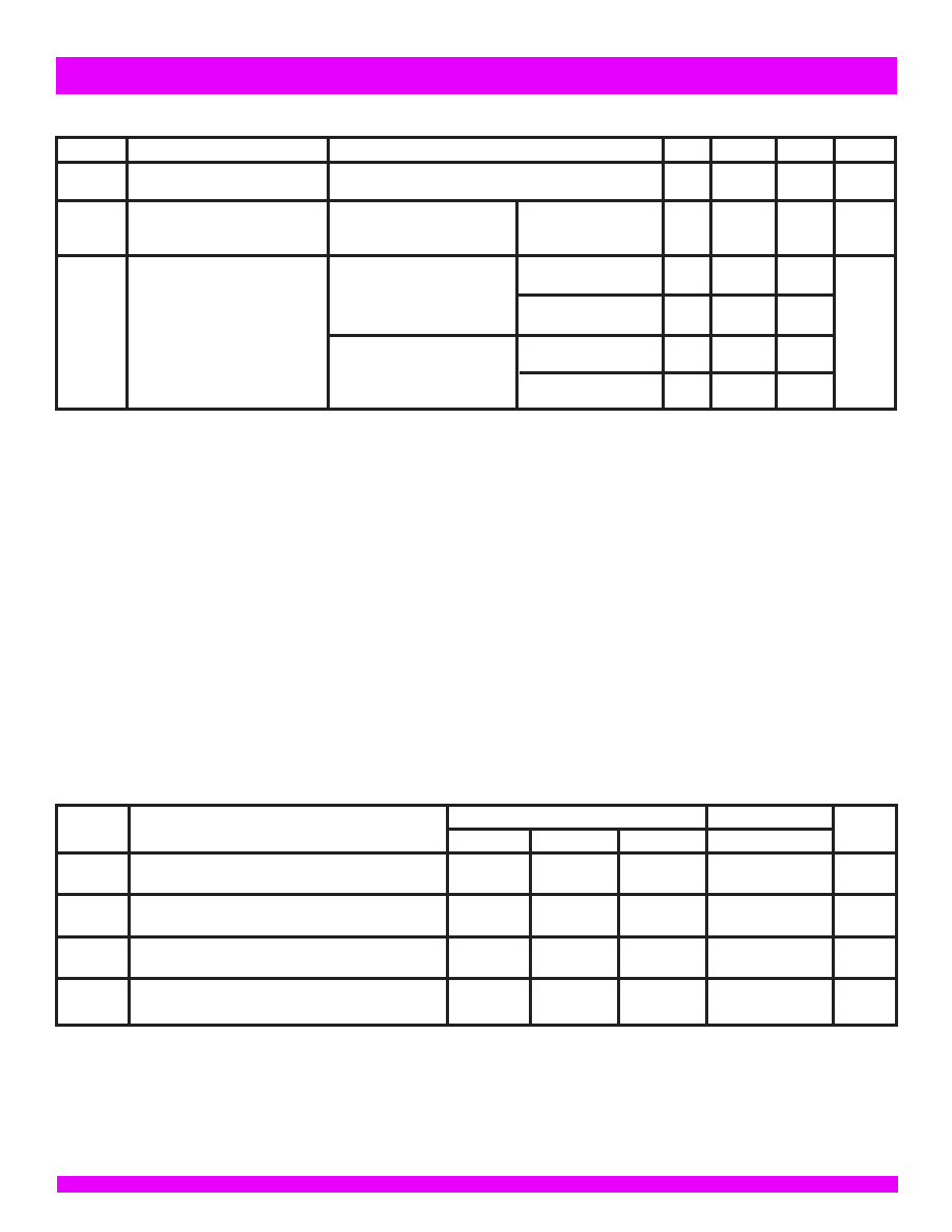
4
INDUSTRIALTEMPERATURERANGE
IDT74FST163210
20-BIT BUS SWITCH
Symbol
Parameter
Test Conditions(1)
Min.
Typ.(2)
Max.
Unit
ICC
Quiescent Power Supply Current
VCC = Max.
—
0.5
1.5
mA
TTL Inputs HIGH
VIN = 3.4V(3)
ICCD
Dynamic Power Supply
VCC = Max.
VIN = VCC
—
120
160
A/
Current(4,5)
One Enable Pin Toggling
VIN = GND
MHz/
50% Duty Cycle
Switch
IC
Total Power Supply Current(6)
VCC = Max.
VIN = VCC
—
1.2
1.6
mA
One Enable Pin Toggling
VIN = GND
fi = 10MHz
VIN = 3.4V
—
1.5
2.4
50% Duty Cycle
VIN = GND
VCC = Max.
VIN = VCC
—
2.4
3.2
Two Enable Pins Toggling
VIN = GND
fi = 10MHz
VIN = 3.4V
—
2.9
4.7
50% Duty Cycle
VIN = GND
POWER SUPPLY CHARACTERISTICS
NOTES:
1. For conditions shown as Max. or Min., use appropriate value specified under Electrical Characteristics for the applicable device type. TA = –40°C to +85°C
2. Typical values are at VCC = 5.0V, +25°C ambient.
3. Per TTL driven input (VIN = 3.4V). All other inputs at VCC or GND. Switch inputs do not contribute to
ICC.
4. This parameter represents the current required to switch the internal capacitance of the control inputs at the specified frequency.
Switch inputs generate no significant power supply currents as they transition. This parameter is not directly testable, but is derived for use in Total Power Supply Calculations.
5. CPD = ICCD/VCC
CPD = Power Dissipation Capacitance
6. IC = IQUIESCENT + IINPUTS + IDYNAMIC
IC = ICC +
ICC DHNT + ICCD (fiN)
ICC = Quiescent Current
ICC = Power Supply Current for a TTL High Input (VIN = 3.4V)
DH = Duty Cycle for TTL Inputs High
NT = Number of TTL Inputs at DH
ICCD = Dynamic Current Caused by an Input Transition Pair (HLH or LHL)
fi = Control Input Frequency
N = Number of Control Inputs Toggling at fi
SWITCHING CHARACTERISTICS OVER OPERATING RANGE
FollowingConditionsApplyUnlessOtherwiseSpecified:
Industrial: TA = -40°C to +85°C, VCC = 5.0V ± 10%
VCC = 5V ± 10%
VCC = 4V
Symbol
Description(1)
Min.
Typ.
Max.
Unit
tPLH
DataPropagationDelay
—
0.25
ns
tPHL
A to B, B to A(2)
tPZH
Switch CONNECT Delay
1.5
—
6.5
—
ns
tPZL
xOE to A or B
tPHZ
Switch DISCONNECT Delay
1.5
—
5.5
—
ns
tPLZ
xOE to A or B
|QCI|
Charge Injection During Switch DISCONNECT
—
1.5
—
pC
xOE to A or B(3)
NOTES:
1. See test circuits and waveforms.
2. The bus switch contributes no Propagation Delay other than the RC Delay of the load interacting with the RC of the switch.
3. |QCI| is the charge injection for a single switch DISCONNECT and applies to either single switches or multiplexers. |QDCI| is the charge injection for a multiplexer as
the multiplexed port switches from one path to another. Charge injection is reduced because the injection from the DISCONNECT of the first path is compensated by
the CONNECT of the second path.
相關PDF資料 |
PDF描述 |
|---|---|
| IDT74FST163211PV8 | CBT/FST/QS/5C/B SERIES, DUAL 12-BIT DRIVER, TRUE OUTPUT, PDSO56 |
| IDT74FST1632383PF8 | CBT/FST/QS/5C/B SERIES, DUAL 10-BIT EXCHANGER, TRUE OUTPUT, PDSO48 |
| IDT74FST163244PV8 | CBT/FST/QS/5C/B SERIES, QUAD 4-BIT DRIVER, TRUE OUTPUT, PDSO48 |
| IDT74FST163292PV | CBT/FST/QS/5C/B SERIES, 24-BIT EXCHANGER, TRUE OUTPUT, PDSO56 |
| IDT74FST163292PA8 | CBT/FST/QS/5C/B SERIES, 24-BIT EXCHANGER, TRUE OUTPUT, PDSO56 |
相關代理商/技術參數(shù) |
參數(shù)描述 |
|---|---|
| IDT74FST163211PV | 制造商:Integrated Device Technology Inc 功能描述: |
| IDT74FST163233PV | 制造商:Integrated Device Technology Inc 功能描述: |
| IDT74FST16323PA | 制造商:Integrated Device Technology Inc 功能描述: |
| IDT74FST163244DPF | 制造商:Rochester Electronics LLC 功能描述:- Bulk 制造商:Integrated Device Technology Inc 功能描述: |
| IDT74FST163244PA | 制造商:INT_DEV_TECH 功能描述: |
發(fā)布緊急采購,3分鐘左右您將得到回復。