- 您現(xiàn)在的位置:買賣IC網(wǎng) > PDF目錄377238 > IDT74FCT841ATE (INTEGRATED DEVICE TECHNOLOGY INC) FAST CMOS BUS INTERFACE LATCHES PDF資料下載
參數(shù)資料
| 型號(hào): | IDT74FCT841ATE |
| 廠商: | INTEGRATED DEVICE TECHNOLOGY INC |
| 元件分類: | 通用總線功能 |
| 英文描述: | FAST CMOS BUS INTERFACE LATCHES |
| 中文描述: | FCT SERIES, 10-BIT DRIVER, TRUE OUTPUT, CDFP24 |
| 封裝: | CERPACK-24 |
| 文件頁(yè)數(shù): | 3/7頁(yè) |
| 文件大?。?/td> | 138K |
| 代理商: | IDT74FCT841ATE |
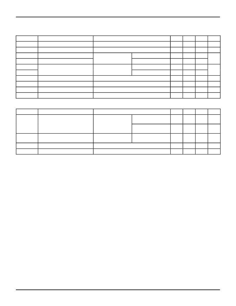
6.22
3
IDT54/74FCT841AT/BT/CT/DT
FAST CMOS BUS INTERFACE LATCHES
MILITARY AND COMMERCIAL TEMPERATURE RANGES
DC ELECTRICAL CHARACTERISTICS OVER OPERATING RANGE
Following Conditions Apply Unless Otherwise Specified:
Commercial: T
A
= 0
°
C to +70
°
C, V
CC
= 5.0V
±
5%; Military: T
A
= –55
°
C to +125
°
C, V
CC
= 5.0V
±
10%
Symbol
Parameter
V
IH
Input HIGH Level
Guaranteed Logic HIGH Level
Test Conditions
(1)
Min.
2.0
Typ.
(2)
—
Max.
—
Unit
V
V
IL
I
I H
I
I L
Input LOW Level
Input HIGH Current
(4)
Input LOW Current
(4)
Guaranteed Logic LOW Level
V
CC
= Max.
—
—
—
—
—
—
0.8
±
1
±
1
±
1
±
1
±
1
–1.2
—
1
V
μ
A
V
I
= 2.7V
V
I
= 0.5V
I
OZH
I
OZL
I
I
High Impedance Output Current
(3-State Output pins)
(4)
Input HIGH Current
(4)
V
CC
= Max.
V
O
= 2.7V
V
O
= 0.5V
—
—
—
—
—
—
μ
A
V
CC
= Max., V
I
= V
CC
(Max.)
μ
A
V
mV
mA
V
IK
V
H
I
CC
Clamp Diode Voltage
Input Hysteresis
Quiescent Power Supply Current
V
CC
= Min., I
IN
= –18mA
—
—
—
–0.7
200
0.01
—
V
CC
= Max., V
IN
= GND or V
CC
2571 lnk 05
Symbol
V
OH
Parameter
Test Conditions
(1)
Min.
2.4
Typ.
(2)
3.3
Max.
—
Unit
V
Output HIGH Voltage
V
CC
= Min.
V
IN
= V
IH
or V
IL
I
OH
= –6mA MIL.
I
OH
= –8mA COM'L.
I
OH
= –12mA MIL.
I
OH
= –15mA COM'L.
I
OL
= 32mA MIL.
I
OL
= 48mA COM'L.
2.0
3.0
—
V
V
OL
Output LOW Voltage
V
CC
= Min.
V
IN
= V
IH
or V
IL
V
CC
= Max., V
O
= GND
(3)
V
CC
= 0V, V
IN
or V
O
≤
4.5V
—
0.3
0.5
V
I
OS
Short Circuit Current
Input/Output Power Off Leakage
(5)
–60
–120
–225
±
1
mA
μ
A
I
OFF
—
—
OUTPUT DRIVE CHARACTERISTICS FOR FCT841T
2571 lnk 06
NOTES:
1. For conditions shown as Max. or Min., use appropriate value specified under Electrical Characteristics for the applicable device type.
2. Typical values are at Vcc = 5.0V, +25
°
C ambient.
3. Not more than one output should be shorted at one time. Duration of the short circuit test should not exceed one second.
4. The test limit for this parameter is
±
5
μ
A at T
A
= –55
°
C.
5. This parameter is guaranteed but not tested.
相關(guān)PDF資料 |
PDF描述 |
|---|---|
| IDT74FCT841ATEB | FAST CMOS BUS INTERFACE LATCHES |
| IDT74FCT841ATL | FAST CMOS BUS INTERFACE LATCHES |
| IDT74FCT841ATLB | FAST CMOS BUS INTERFACE LATCHES |
| IDT74FCT841ATP | FAST CMOS BUS INTERFACE LATCHES |
| IDT74FCT841ATPB | FAST CMOS BUS INTERFACE LATCHES |
相關(guān)代理商/技術(shù)參數(shù) |
參數(shù)描述 |
|---|---|
| IDT74FCT841ATSO | 制造商:Integrated Device Technology Inc 功能描述: |
| IDT74FCT841BP | 制造商:Integrated Device Technology Inc 功能描述: |
| IDT74FCT841BTSO | 制造商:Integrated Device Technology Inc 功能描述: |
| IDT74FCT841HAP | 制造商:Rochester Electronics LLC 功能描述:- Bulk |
| IDT74FCT841HATP | 制造商:Integrated Device Technology Inc 功能描述: |
發(fā)布緊急采購(gòu),3分鐘左右您將得到回復(fù)。