- 您現(xiàn)在的位置:買賣IC網 > PDF目錄377241 > IDT6116SA25YB (Integrated Device Technology, Inc.) CMOS STATIC RAM 16K (2K x 8 BIT) PDF資料下載
參數(shù)資料
| 型號: | IDT6116SA25YB |
| 廠商: | Integrated Device Technology, Inc. |
| 英文描述: | CMOS STATIC RAM 16K (2K x 8 BIT) |
| 中文描述: | 的CMOS靜態(tài)RAM 16K的(2K × 8位) |
| 文件頁數(shù): | 2/10頁 |
| 文件大?。?/td> | 91K |
| 代理商: | IDT6116SA25YB |
5.1
2
IDT6116SA/LA
CMOS STATIC RAM 16K (2K x 8-BIT)
MILITARY AND COMMERCIAL TEMPERATURE RANGES
PIN CONFIGURATIONS
ABSOLUTE MAXIMUM RATINGS
(1)
Symbol
Rating
Terminal Voltage
V
TERM
(2)
with Respect to GND –0.5 to + 7.0 –0.5 to +7.0
Operating
T
A
Temperature
Temperature
T
BIAS
Under Bias
Storage
T
STG
Temperature
Power
P
T
Dissipation
I
OUT
DC Output Current
NOTES:
1. Stresses greater than those listed under ABSOLUTE MAXIMUM RAT-
INGS may cause permanent damage to the device. This is a stress rating
only and functional operation of the device at these or any other conditions
above those indicated in the operational sections of this specification is not
implied. Exposure to absolute maximum rating conditions for extended
periods may affect reliability.
2. V
TERM
must not exceed V
CC
+0.5V.
Commercial
Military
Unit
V
0 to + 70
–55 to +125
°
C
–55 to + 125 –65 to +135
°
C
–55 to + 125 –65 to +150
°
C
1.0
50
1.0
50
W
mA
3089 tbl 04
TRUTH TABLE
(1)
Mode
Standby
Read
Read
Write
NOTE:
1. H = V
IH
, L = V
IL
, X = Don't Care.
CS
OE
WE
I/O
H
L
L
L
X
L
H
X
X
H
H
L
High-Z
DATA
OUT
High-Z
DATA
IN
3089 tbl 02
PIN DESCRIPTIONS
A
0
–A
13
I/O
0
–I/O
7
CS
Address Inputs
Data Input/Output
Chip Select
Write Enable
Output Enable
Power
Ground
WE
OE
V
CC
GND
3089 tbl 01
CAPACITANCE
(T
A
= +25
°
C, F = 1.0 MH
Z
)
Symbol
Parameter
(1)
C
IN
Input Capacitance
C
I/O
I/O Capacitance
NOTE:
1. This parameter is determined by device characterization, but is not
production tested.
Conditions
V
IN
= 0V
V
OUT
= 0V
Max.
8
8
Unit
pF
pF
3089 tbl 03
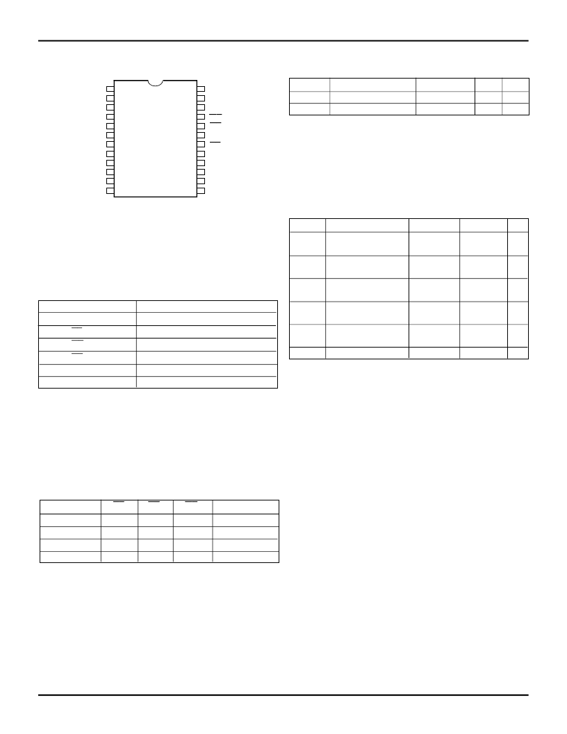
DIP/SOIC/SOJ
TOP VIEW
3089 drw 02
5
6
7
8
9
10
11
12
GND
1
2
3
4
24
23
22
21
20
19
18
17
16
15
14
13
P24-2
P24-1
D24-2
D24-1
SO24-2
&
S024-4
A
5
A
4
A
3
A
2
A
1
A
0
I/O
0
I/O
1
I/O
2
V
CC
A
8
A
9
WE
OE
A
10
CS
I/O
5
I/O
4
I/O
3
A
7
A
6
I/O
7
I/O
6
相關PDF資料 |
PDF描述 |
|---|---|
| IDT6116LA25YB | CMOS STATIC RAM 16K (2K x 8 BIT) |
| IDT6116LA120D | CMOS STATIC RAM 16K (2K x 8 BIT) |
| IDT6116LA120DB | CMOS STATIC RAM 16K (2K x 8 BIT) |
| IDT6116LA120P | CMOS STATIC RAM 16K (2K x 8 BIT) |
| IDT6116LA | CMOS STATIC RAM 16K (2K x 8 BIT) |
相關代理商/技術參數(shù) |
參數(shù)描述 |
|---|---|
| IDT6116SA25YI | 制造商:IDT 制造商全稱:Integrated Device Technology 功能描述:CMOS STATIC RAM 16K (2K x 8 BIT) |
| IDT6116SA30D | 制造商:未知廠家 制造商全稱:未知廠家 功能描述:x8 SRAM |
| IDT6116SA30E | 制造商:未知廠家 制造商全稱:未知廠家 功能描述:x8 SRAM |
| IDT6116SA30F | 制造商:未知廠家 制造商全稱:未知廠家 功能描述:x8 SRAM |
| IDT6116SA30L24 | 制造商:未知廠家 制造商全稱:未知廠家 功能描述:x8 SRAM |
發(fā)布緊急采購,3分鐘左右您將得到回復。