- 您現(xiàn)在的位置:買賣IC網(wǎng) > PDF目錄377225 > IDT54FCT823CTP (Integrated Device Technology, Inc.) HIGH-PERFORMANCE CMOS BUS INTERFACE REGISTERS PDF資料下載
參數(shù)資料
| 型號: | IDT54FCT823CTP |
| 廠商: | Integrated Device Technology, Inc. |
| 英文描述: | HIGH-PERFORMANCE CMOS BUS INTERFACE REGISTERS |
| 中文描述: | 高性能CMOS總線接口寄存器 |
| 文件頁數(shù): | 3/9頁 |
| 文件大?。?/td> | 178K |
| 代理商: | IDT54FCT823CTP |
IDT54/74FCT821AT/BT/CT, 823/825AT/BT/CT/DT
HIGH-PERFORMANCE CMOS BUS INTERFACE REGISTERS
MILITARY AND COMMERCIAL TEMPERATURE RANGES
6.21
3
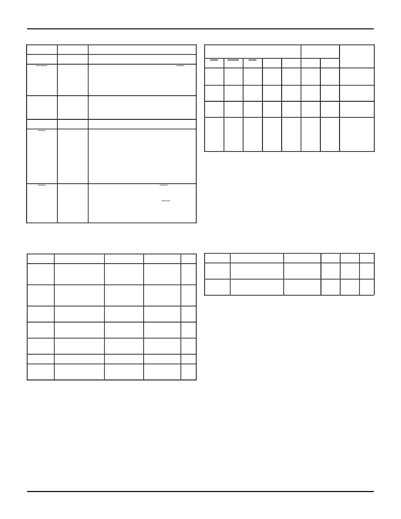
FUNCTION TABLE
(1)
PIN DESCRIPTION
2567 tbl 01
ABSOLUTE MAXIMUM RATINGS
(1)
CAPACITANCE
(
T
A
= +25
°
C, f = 1.0MHz)
Symbol
Parameter
(1)
C
IN
Input
Capacitance
C
OUT
Output
Capacitance
Symbol
V
TERM(2)
Terminal Voltage
with Respect to
GND
V
TERM(3)
Terminal Voltage
with Respect to
GND
T
A
Operating
Temperature
T
BIAS
Temperature
Under Bias
T
STG
Storage
Temperature
P
T
Power Dissipation
Rating
Commercial
–0.5 to +7.0
Military
–0.5 to +7.0
Unit
V
–0.5 to
V
CC
+0.5
–0.5 to
V
CC
+0.5
V
0 to +70
–55 to +125
°
C
–55 to +125
–65 to +135
°
C
–55 to +125
–65 to +150
°
C
0.5
0.5
W
I
OUT
DC Output
Current
–60 to +120 –60 to +120 mA
NOTES:
1. Stresses greater than those listed under ABSOLUTE MAXIMUM RAT-
INGS may cause permanent damage to the device. This is a stress rating
only and functional operation of the device at these or any other conditions
above those indicated in the operational sections of this specification is
not
implied. Exposure to absolute maximum rating conditions for
extended periods may affect reliability. No terminal voltage may exceed
V
CC
by +0.5V unless otherwise noted.
2. Input and V
CC
terminals only.
3. Outputs and I/O terminals only.
NOTE:
1. This parameter is measured at characterization but not tested.
2567 lnk 03
2567 lnk 04
Conditions
V
IN
= 0V
Typ.
6
Max. Unit
10
pF
V
OUT
= 0V
8
12
pF
Inputs
Internal/
Outputs
Q
I
L
H
OE
CLR
EN
D
I
L
H
CP
↑
↑
X
X
X
X
↑
↑
↑
↑
Y
I
Z
Z
Function
High Z
H
H
H
H
L
L
H
L
H
L
H
H
L
L
L
L
H
H
H
H
H
H
X
X
H
H
L
L
L
L
X
X
X
X
L
H
L
H
L
L
Z
L
Z
Clear
NC
NC
L
H
L
H
NC
Z
Z
L
H
Hold
Load
Names
D
I
CLR
I/O
I
I
Description
The D flip-flop data inputs.
When the clear input is LOW and
OE
is
LOW, the Q
I
outputs are LOW. When
the clear input is HIGH, data can be
entered into the register.
Clock Pulse for the Register; enters
data into the register on the LOW-to-
HIGH transition.
The register 3-state outputs.
Clock Enable. When the clock enable is
LOW, data on the D
I
input is transferred
to the Q
I
output on the LOW-to-HIGH
clock transition. When the clock enable
is HIGH, the Q
I
outputs do not change
state, regardless of the data or clock
input transitions.
Output Control. When the
OE
input is
HIGH, the Y
impedance state. When the
OE
input is
LOW, the TRUE register data is present
at the Y
I
outputs.
CP
I
Y
I
EN
O
I
OE
I
outputs are in the high-
NOTE:
1. H = HIGH
L = LOW
X = Don’t Care
NC = No Change
↑
= LOW-to-HIGH Transition
Z = High Impedance
2567 tbl 02
相關(guān)PDF資料 |
PDF描述 |
|---|---|
| IDT54FCT823CTPB | Ceramic Chip Capacitors / Standard X7R; Capacitance [nom]: 4.7uF; Working Voltage (Vdc)[max]: 6.3V; Capacitance Tolerance: +/-20%; Dielectric: Multilayer Ceramic; Temperature Coefficient: X7R; Lead Style: Surface Mount Chip; Lead Dimensions: 1210; Termination: Tin Plated Nickel Barrier; Body Dimensions: 0.126" x 0.098"; Container: Bulk; Features: Unmarked |
| IDT54FCT823CTPY | HIGH-PERFORMANCE CMOS BUS INTERFACE REGISTERS |
| IDT54FCT823CTPYB | HIGH-PERFORMANCE CMOS BUS INTERFACE REGISTERS |
| IDT54FCT823CTQ | HIGH-PERFORMANCE CMOS BUS INTERFACE REGISTERS |
| IDT54FCT823CTQB | HIGH-PERFORMANCE CMOS BUS INTERFACE REGISTERS |
相關(guān)代理商/技術(shù)參數(shù) |
參數(shù)描述 |
|---|---|
| IDT54FCT845ADB | 制造商:Integrated Device Technology Inc 功能描述: |
| IDT54FCT861ADB | 制造商:Integrated Device Technology Inc 功能描述: |
| IDT54FCT861BDB | 制造商:Integrated Device Technology Inc 功能描述: |
| IDT557GI-05ALF | 制造商: 功能描述: 制造商:undefined 功能描述: |
| IDT557GI-06LF | 制造商: 功能描述: 制造商:undefined 功能描述: |
發(fā)布緊急采購,3分鐘左右您將得到回復(fù)。