- 您現(xiàn)在的位置:買賣IC網(wǎng) > PDF目錄377231 > IDT54FCT2827CTP (Integrated Device Technology, Inc.) FAST CMOS 10-BIT BUFFERS PDF資料下載
參數(shù)資料
| 型號: | IDT54FCT2827CTP |
| 廠商: | Integrated Device Technology, Inc. |
| 英文描述: | FAST CMOS 10-BIT BUFFERS |
| 中文描述: | 快速CMOS 10位緩沖器 |
| 文件頁數(shù): | 1/7頁 |
| 文件大小: | 127K |
| 代理商: | IDT54FCT2827CTP |
IDT54/74FCT827AT/BT/CT/DT, IDT54/74FCT2827AT/BT/CT
HIGH-PERFORMANCE CMOS BUFFERS
MILITARY AND COMMERCIAL TEMPERATURE RANGES
6.22
Integrated Device Technology, Inc.
MILITARY AND COMMERCIAL TEMPERATURE RANGES
AUGUST 1995
1995 Integrated Device Technology, Inc.
6.22
DSC-4217/5
1
FAST CMOS 10-BIT
BUFFERS
DESCRIPTION:
The FCT827T is built using an advanced dual metal CMOS
technology.
The FCT827T/FCT2827T 10-bit bus drivers provide high-
performance bus interface buffering for wide data/address
paths or buses carrying parity. The 10-bit buffers have NAND-
ed output enables for maximum control flexibility.
All of the FCT827T high-performance interface family are
designed for high-capacitance load drive capability, while
providing low-capacitance bus loading at both inputs and
outputs. All inputs have clamp diodes to ground and all outputs
are designed for low-capacitance bus loading in high-imped-
ance state.
The FCT2827T has balanced output drive with current
limiting resistors. This offers low ground bounce, minimal
undershoot and controlled output fall times-reducing the need
for external series terminating resistors. FCT2827T parts are
plug-in replacements for FCT827T parts.
IDT54/74FCT827AT/BT/CT/DT
IDT54/74FCT2827AT/BT/CT
FEATURES:
Common features:
–
Low input and output leakage
≤
1
μ
A (max.)
–
CMOS power levels
–
True TTL input and output compatibility
– V
OH
= 3.3V (typ.)
– V
OL
= 0.3V (typ.)
–
Meets or exceeds JEDEC standard 18 specifications
–
Product available in Radiation Tolerant and Radiation
Enhanced versions
–
Military product compliant to MIL-STD-883, Class B
and DESC listed (dual marked)
–
Available in DIP, SOIC, SSOP, QSOP, CERPACK
and LCC packages
Features for FCT827T:
–
A, B, C and D speed grades
–
High drive outputs (-15mA I
OH
, 48mA I
OL
)
Features for FCT2827T:
–
A, B and C speed grades
–
Resistor outputs
(-15mA I
OH
, 12mA I
OL
Com.)
(-12mA I
OH
, 12mA I
OL
Mil.)
–
Reduced system switching noise
The IDT logo is a registered trademark of Integrated Device Technology, Inc.
2573 drw 01
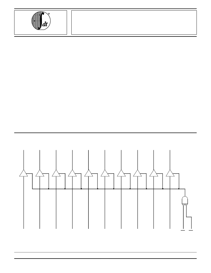
D
0
D
1
D
2
D
3
D
4
D
5
D
6
D
7
D
8
D
9
OE
1
OE
2
Y
0
Y
1
Y
2
Y
3
Y
4
Y
5
Y
6
Y
7
Y
8
Y
9
FUNCTIONAL BLOCK DIAGRAM
相關(guān)PDF資料 |
PDF描述 |
|---|---|
| IDT54FCT2827CTPB | FAST CMOS 10-BIT BUFFERS |
| IDT54FCT2827CTPY | FAST CMOS 10-BIT BUFFERS |
| IDT54FCT2827CTPYB | FAST CMOS 10-BIT BUFFERS |
| IDT54FCT2827CTQ | FAST CMOS 10-BIT BUFFERS |
| IDT54FCT2827CTQB | FAST CMOS 10-BIT BUFFERS |
相關(guān)代理商/技術(shù)參數(shù) |
參數(shù)描述 |
|---|---|
| IDT54FCT299ADB | 制造商:Integrated Device Technology Inc 功能描述: |
| IDT54FCT299DB | 制造商:Integrated Device Technology Inc 功能描述:Shift Register, 20 Pin, Ceramic, DIP |
| IDT54FCT299TLB | 制造商:Integrated Device Technology Inc 功能描述: |
| IDT54FCT373ATDB | 制造商:Integrated Device Technology Inc 功能描述: 制造商:Integrated Device Technology Inc 功能描述:IC TXRX OCTAL BIDIRECT 20CERDIP |
| IDT54FCT373ATLB | 制造商:Integrated Device Technology Inc 功能描述: 制造商:Integrated Device Technology Inc 功能描述:IC TXRX OCTAL BIDIRECT 20LCC |
發(fā)布緊急采購,3分鐘左右您將得到回復(fù)。