- 您現(xiàn)在的位置:買賣IC網(wǎng) > PDF目錄65575 > IDT54FCT2244ATDB (INTEGRATED DEVICE TECHNOLOGY INC) FCT SERIES, DUAL 4-BIT DRIVER, TRUE OUTPUT, CDIP20 PDF資料下載
參數(shù)資料
| 型號: | IDT54FCT2244ATDB |
| 廠商: | INTEGRATED DEVICE TECHNOLOGY INC |
| 元件分類: | 總線收發(fā)器 |
| 英文描述: | FCT SERIES, DUAL 4-BIT DRIVER, TRUE OUTPUT, CDIP20 |
| 封裝: | CERDIP-20 |
| 文件頁數(shù): | 4/6頁 |
| 文件大?。?/td> | 125K |
| 代理商: | IDT54FCT2244ATDB |
4
MILITARYANDINDUSTRIALTEMPERATURERANGES
IDT54/74FCT2244T/AT/CT
FASTCMOSOCTALBUFFER/LINEDRIVER
NOTES:
1. For conditions shown as Max. or Min., use appropriate value specified under Electrical Characteristics for the applicable device type.
2. Typical values are at VCC = 5.0V, +25°C ambient.
3. Per TTL driven input (VIN = 3.4V). All other inputs at VCC or GND.
4. This parameter is not directly testable, but is derived for use in Total Power Supply Calculations.
5. Values for these conditions are examples of the ICC formula. These limits are guaranteed but not tested.
6. IC = IQUIESCENT + IINPUTS + IDYNAMIC
IC = ICC +
ICC DHNT + ICCD (fCP/2 + fiNi)
ICC = Quiescent Current
ICC = Power Supply Current for a TTL High Input (VIN = 3.4V)
DH = Duty Cycle for TTL Inputs High
NT = Number of TTL Inputs at DH
ICCD = Dynamic Current Caused by an Input Transition Pair (HLH or LHL)
fCP = Clock Frequency for Register Devices (Zero for Non-Register Devices)
fi = Input Frequency
Ni = Number of Inputs at fi
All currents are in milliamps and all frequencies are in megahertz.
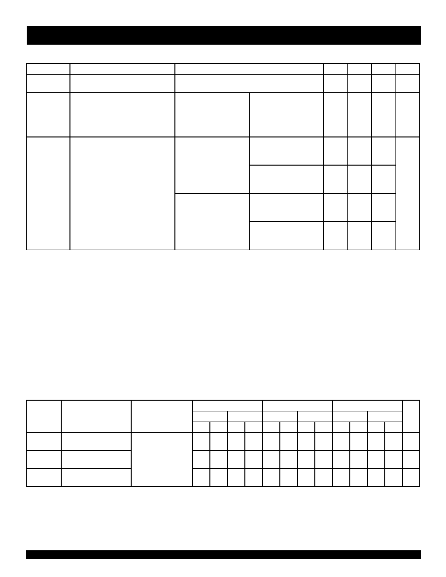
POWER SUPPLY CHARACTERISTICS
Symbol
Parameter
Test Conditions(1)
Min.
Typ.(2)
Max.
Unit
ICC
Quiescent Power Supply Current
TTL Inputs HIGH
VCC = Max.
VIN = 3.4V(3)
—0.5
2
mA
ICCD
Dynamic Power Supply Current(4)
VCC = Max.
Outputs Open
OEA = OEB = GND
VIN = VCC
VIN = GND
—
0.06
0.12
mA/
MHz
One Input Toggling
50% Duty Cycle
IC
Total Power Supply Current(6)
VCC = Max.
VIN = VCC
—0.6
2.2
mA
Outputs Open
fi = 10MHz
VIN = GND
50% Duty Cycle
OEA = OEB = GND
VIN = 3.4
VIN = GND
—0.9
3.2
One Bit Toggling
VCC = Max.
VIN = VCC
—1.2
3.4(5)
Outputs Open
fi = 2.5MHz
VIN = GND
50% Duty Cycle
OEA = OEB = GND
VIN = 3.4
VIN = GND
—
3.2
11.4(5)
Eight Bits Toggling
SWITCHING CHARACTERISTICS OVER OPERATING RANGE
FCT2244T
FCT2244AT
FCT2244CT
Ind.
Mil.
Ind.
Mil.
Ind.
Mil.
Symbol
Parameter
Condition(1)
Min.(2) Max. Min.(2) Max. Min.(2) Max. Min.(2) Max. Min.(2) Max. Min.(2) Max.
Unit
tPLH
tPHL
Propagation Delay
DN to ON
CL = 50pF
RL = 500
1.5
6.5
1.5
7
1.5
4.8
1.5
5.1
1.5
4.1
1.5
4.6
ns
tPZH
tPZL
Output Enable Time
1.5
8
1.5
8.5
1.5
6.2
1.5
6.5
1.5
5.8
1.5
6.5
ns
tPHZ
tPLZ
Output Disable Time
1.5
7
1.5
7.5
1.5
5.6
1.5
5.9
1.5
5.2
1.5
5.7
ns
NOTES:
1. See Test Circuit and Waveforms.
2. Minimum limits are guaranteed but not tested on Propagation Delays.
相關PDF資料 |
PDF描述 |
|---|---|
| IDT54FCT244CTEB | FCT SERIES, DUAL 4-BIT DRIVER, TRUE OUTPUT, CDFP20 |
| IDT54FCT3245EB | FCT SERIES, 8-BIT TRANSCEIVER, TRUE OUTPUT, CDFP20 |
| IDT54FCT3245ALB | FCT SERIES, 8-BIT TRANSCEIVER, TRUE OUTPUT, CQCC20 |
| IDT54FCT3245ADB | FCT SERIES, 8-BIT TRANSCEIVER, TRUE OUTPUT, CDIP20 |
| IDT54FCT3245LB | FCT SERIES, 8-BIT TRANSCEIVER, TRUE OUTPUT, CQCC20 |
相關代理商/技術參數(shù) |
參數(shù)描述 |
|---|---|
| IDT54FCT2374KATEB | 制造商:Rochester Electronics LLC 功能描述:- Bulk |
| IDT54FCT240ATDB | 制造商:Integrated Device Technology Inc 功能描述:IC TXRX 16BIT BIDIRECT 20CERPACK |
| IDT54FCT240ATLB | 制造商:Integrated Device Technology Inc 功能描述: 制造商:Integrated Device Technology Inc 功能描述:IC TXRX 16BIT BIDIRECT 20LCC |
| IDT54FCT240CTDB | 制造商:Integrated Device Technology Inc 功能描述:IC TXRX 16BIT BIDIRECT 20CERDIP |
| IDT54FCT240CTLB | 制造商:Integrated Device Technology Inc 功能描述:IC TXRX 16BIT BIDIRECT 20LCC |
發(fā)布緊急采購,3分鐘左右您將得到回復。