- 您現(xiàn)在的位置:買賣IC網(wǎng) > PDF目錄360752 > ICS650-11B BroadCom Networking Clock Synthesizer PDF資料下載
參數(shù)資料
| 型號(hào): | ICS650-11B |
| 英文描述: | BroadCom Networking Clock Synthesizer |
| 中文描述: | 博通網(wǎng)絡(luò)時(shí)鐘合成器 |
| 文件頁(yè)數(shù): | 3/4頁(yè) |
| 文件大?。?/td> | 50K |
| 代理商: | ICS650-11B |
ICS650-11B
BroadCom Networking Clock Synthesizer
MDS 650-11B
C
Integrated Circuit Systems, Inc. 525 Race Street San Jose CA 95126(408)295-9800tel www.icst.com
3
Revision
012005
Printed 11/1
4/04
PRELIMINARY INFORMATION
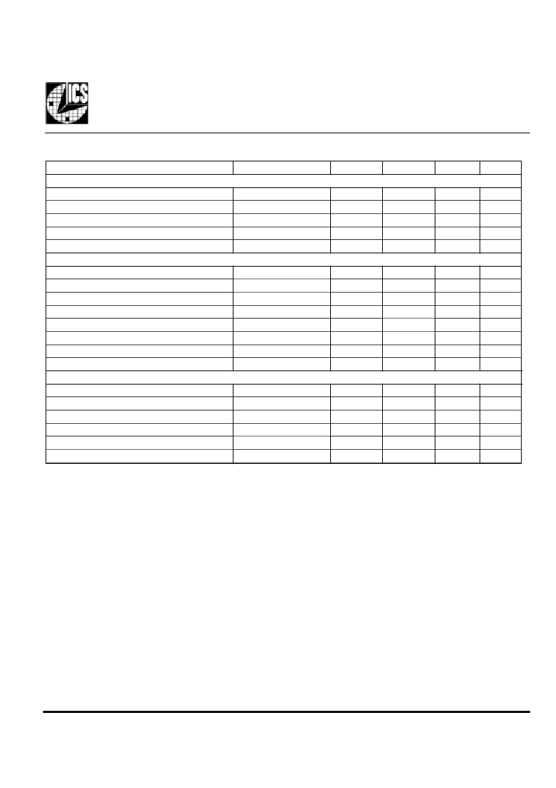
Parameter
ABSOLUTE MAXIMUM RATINGS (note 1)
Supply voltage, VDD
Inputs and Clock Outputs
Ambient Operating Temperature
Soldering Temperature
Storage temperature
DC CHARACTERISTICS (VDD = 3.3V unless noted)
Operating Voltage, VDD
Input High Voltage, VIH, X1 pin only
Input Low Voltage, VIL, X1 pin only
Output High Voltage, VOH
Output Low Voltage, VOL
Output High Voltage, VOH, CMOS level
Operating Supply Current, IDD
Short Circuit Current
AC CHARACTERISTICS (VDD = 3.3V unless noted)
Input Frequency
Output Clock Rise Time
Output Clock Fall Time
Output Clock Duty Cycle, except 25 MHz
Frequency error
Absolute Jitter, short term
Conditions
Minimum
Typical
Maximum
Units
Referenced to GND
Referenced to GND
7
V
V
°C
°C
°C
-0.5
-40
VDD+0.5
85
260
150
Max of 20 seconds
-65
3
5.5
V
V
V
V
V
V
VDD/2 + 1
VDD/2
VDD/2
VDD/2 - 1
IOH=-12mA
IOL=12mA
IOH=-8mA
No Load
Each output
2.4
0.4
VDD-0.4
35
±50
mA
mA
25.000
MH z
ns
ns
%
ppm
ps
0.8 to 2.0V
2.0 to 0.8V
At VDD/2
All clocks
Variation from mean
1.5
1.5
55
0
45
50
175
Electrical Specifications
Notes:
1. Stresses beyond those listed under Absolute Maximum Ratings could cause permanent damage to the device. Prolonged
exposure to levels above the operating limits but below the Absolute Maximums may affect device reliability.
External Components
The ICS650-11B requires a minimum number of external components for proper operation. Decoupling
capacitors of 0.01μF should be connected between each VDD and GND on Pins 4 and 6, and Pins 16 and
14, as close to the ICS650-11B as possible. A series termination resistor of 33
may be used for each clock
output. The 25.00 MHz crystal must be connected as close to the chip as possible. The crystal should be a
fundamental mode (do not use third overtone), parallel resonant. Crystal capacitors should be connected
from pins X1 to ground and X2 to ground to optimize the initial accuracy. The value of these capacitors is
given by the following equation, where C
L
is the crystal load capacitance: Crystal caps (pF) = (C
L
-6) x 2. So
for a crystal with 16 pF load capacitance, two 20 pF caps should be used.
相關(guān)PDF資料 |
PDF描述 |
|---|---|
| ICS650R-11I | BroadCom Networking Clock Synthesizer |
| ICS650R-11IT | BroadCom Networking Clock Synthesizer |
| ICS650-14B | Networking System Clock |
| ICS650-22 | PVR and STB Clock Source |
| ICS650R-22 | PVR and STB Clock Source |
相關(guān)代理商/技術(shù)參數(shù) |
參數(shù)描述 |
|---|---|
| ICS650-12 | 制造商:ICS 制造商全稱:ICS 功能描述:MPEG Clock Synthesizer |
| ICS650-14B | 制造商:ICS 制造商全稱:ICS 功能描述:Networking System Clock |
| ICS650-21 | 制造商:ICS 制造商全稱:ICS 功能描述:System Peripheral Clock Source |
| ICS650-22 | 制造商:ICS 制造商全稱:ICS 功能描述:PVR and STB Clock Source |
| ICS650-27 | 制造商:ICS 制造商全稱:ICS 功能描述:Networking Clock Source |
發(fā)布緊急采購(gòu),3分鐘左右您將得到回復(fù)。