- 您現(xiàn)在的位置:買賣IC網(wǎng) > PDF目錄65530 > ICS5OSK481TILF (INTEGRATED DEVICE TECHNOLOGY INC) 5OSK SERIES, PLL BASED CLOCK DRIVER, 1 TRUE OUTPUT(S), 0 INVERTED OUTPUT(S), PDSO5 PDF資料下載
參數(shù)資料
| 型號: | ICS5OSK481TILF |
| 廠商: | INTEGRATED DEVICE TECHNOLOGY INC |
| 元件分類: | 時鐘及定時 |
| 英文描述: | 5OSK SERIES, PLL BASED CLOCK DRIVER, 1 TRUE OUTPUT(S), 0 INVERTED OUTPUT(S), PDSO5 |
| 封裝: | ROHS COMPLIANT, TSOT-5 |
| 文件頁數(shù): | 2/6頁 |
| 文件大小: | 212K |
| 代理商: | ICS5OSK481TILF |
48 MHz Tiny USB Clock Source
MDS 5OSK481 B
2
Revision 111805
Integrated Circuit Systems, Inc.
● 525 Race Street, San Jose, CA 95126 ● tel (408) 297-1201 ● www.icst.com
PRELIM INAR Y INFORM A T ION
ICS5OSK481
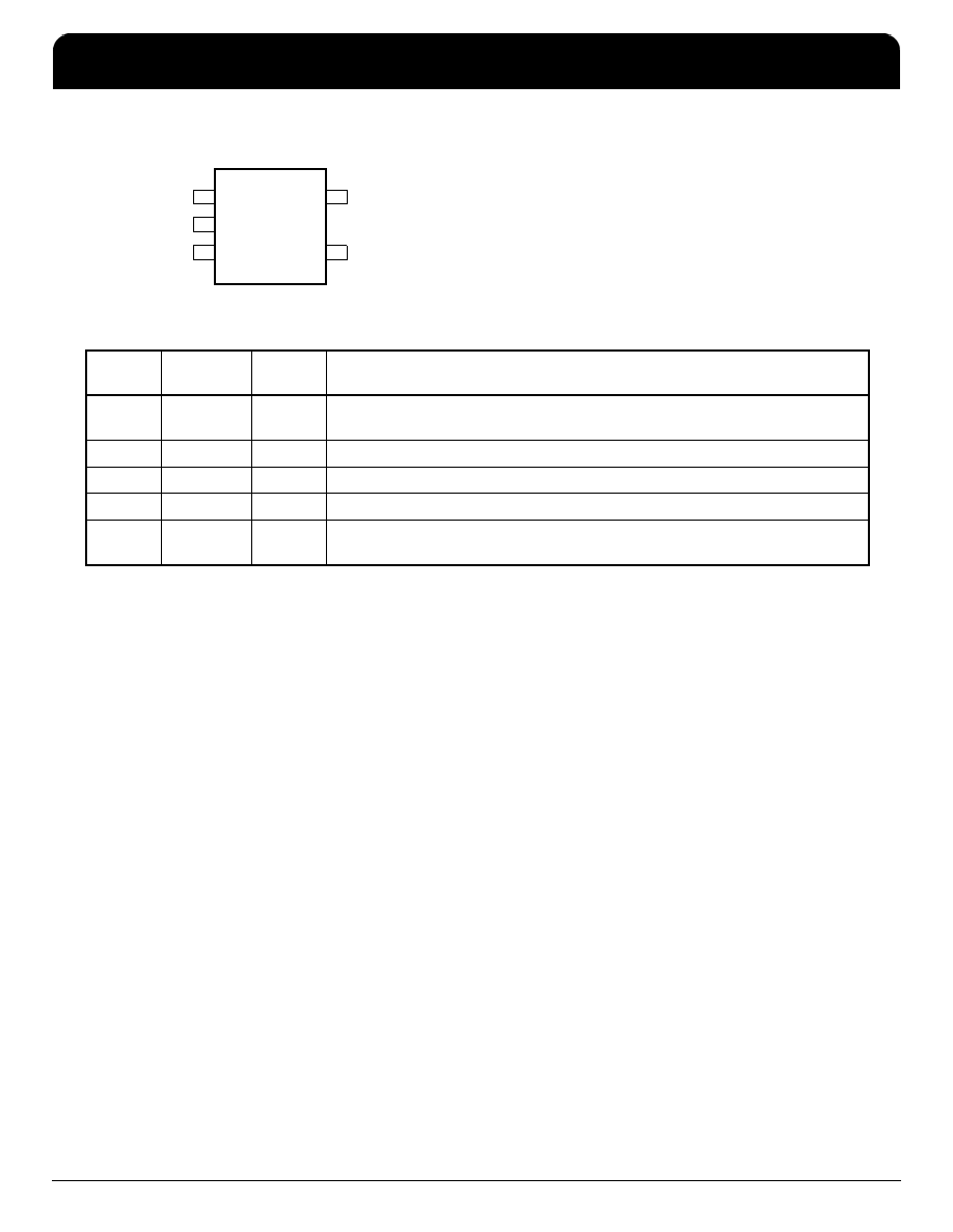
Pin Assignment
Pin Descriptions
External Components
Decoupling Capacitor
As with any high-performance mixed-signal IC, the
ICS5OSK481 must be isolated from system power
supply noise to perform optimally.
A decoupling capacitor of 0.01F must be connected
between each VDD and the PCB ground plane.
Series Termination Resistor
Clock output traces over one inch should use series
termination. To series terminate a 50
trace (a
commonly used trace impedance), place a 33
resistor
in series with the clock line, as close to the clock output
pin as possible. The nominal impedance of the clock
output is 20
.
PCB Layout Recommendations
For optimum device performance and lowest output
phase noise, the following guidelines should be
observed.
1) The 0.01F decoupling capacitors should be
mounted on the component side of the board as close
to the VDD pin as possible. No vias should be used
between the decoupling capacitors and VDD pins. The
PCB trace to VDD pins should be kept as short as
possible, as should the PCB trace to the ground via.
2) To minimize EMI, the 33
series termination resistor
(if needed) should be placed close to the clock output.
3) An optimum layout is one with all components on the
same side of the board, minimizing vias through other
signal layers. Other signal traces should be routed
away from the ICS5OSK481. This includes signal
traces just underneath the device, or on layers adjacent
to the ground plane layer used by the device.
OE
GN D
CLK
ICLK
1
2
3
5
4
VDD
Pin
Number
Pin
Name
Pin
Type
Pin Description
1
ICLK
Input
25 MHz clock input. Connect to a parallel resonant fundamental crystal or
input clock.
2
GND
Power
Connect to ground.
3
CLK
Output
PLL output clock. Internal pull-down resistor.
4
VDD
Power
Connect to 3.3 V.
5
OE
Input
Output Enable pin. Internal pull-up resistor. OE=0 outputs tristate with weak
pull-down.
ICS5OSK481
48 MHz Tiny USB Clock Source
TSD
IDT / ICS 48 MHz Tiny USB Clock Source
ICS5OSK481
2
相關PDF資料 |
PDF描述 |
|---|---|
| ICS601G-21LFT | 220 MHz, OTHER CLOCK GENERATOR, PDSO16 |
| ICS601G-21T | 220 MHz, OTHER CLOCK GENERATOR, PDSO16 |
| ICS601M-01T | 156 MHz, OTHER CLOCK GENERATOR, PDSO16 |
| ICS601G-01IT | 156 MHz, OTHER CLOCK GENERATOR, PDSO16 |
| ICS601G-01ILF | 156 MHz, OTHER CLOCK GENERATOR, PDSO16 |
相關代理商/技術參數(shù) |
參數(shù)描述 |
|---|---|
| ICS5OSK481TILFT | 制造商:ICS 制造商全稱:ICS 功能描述:48 MHz Tiny USB Clock Source |
| ICS5OSK482 | 制造商:ICS 制造商全稱:ICS 功能描述:48 MHz Tiny USB Clock Source |
| ICS5OSK482TILF | 制造商:ICS 制造商全稱:ICS 功能描述:48 MHz Tiny USB Clock Source |
| ICS5OSK482TILFT | 制造商:ICS 制造商全稱:ICS 功能描述:48 MHz Tiny USB Clock Source |
| ICS601 | 制造商:ICS 制造商全稱:ICS 功能描述:ICS601 Demo Board Schematic |
發(fā)布緊急采購,3分鐘左右您將得到回復。