- 您現(xiàn)在的位置:買賣IC網(wǎng) > PDF目錄360751 > ICS581G-02T Linear Voltage Regulators for Automotive Applications; Package: PG-DSO-14; Regulator Type: single output; Output Voltage: 5V; Accuracy: 2.0 %; Max. Output Current: 150mA; Dropout Voltage: 250mV PDF資料下載
參數(shù)資料
| 型號(hào): | ICS581G-02T |
| 元件分類: | 基準(zhǔn)電壓源/電流源 |
| 英文描述: | Linear Voltage Regulators for Automotive Applications; Package: PG-DSO-14; Regulator Type: single output; Output Voltage: 5V; Accuracy: 2.0 %; Max. Output Current: 150mA; Dropout Voltage: 250mV |
| 中文描述: | 零延遲無干擾時(shí)鐘復(fù)用器 |
| 文件頁數(shù): | 5/6頁 |
| 文件大小: | 92K |
| 代理商: | ICS581G-02T |
ICS581-01, -02
Zero-Delay Glitch-Free Clock Multiplexer
MDS 581-01, 581-02 A
Integrated Circuit Systems, Inc. 525 Race Street San Jose CA95126 (408) 295-9800tel www.icst.com
5
Revision 041100
Printed 11/14/00
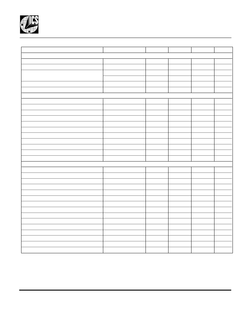
Parameter
ABSOLUTE MAXIMUM RATINGS
Supply voltage, VDD
Inputs and Clock Outputs
Ambient Operating Temperature
Conditions
Minimum
Typical
Maximum
Units
Referenced to GND
Referenced to GND
7
V
V
°C
°C
°C
°C
-0.5
0
-40
VDD+0.5
70
85
260
150
ICS581G-01I
Max of 10 seconds
Soldering Temperature
Storage temperature
DC CHARACTERISTICS (VDD = 3.3 V unless noted)
Operating Voltage, VDD
Input High Voltage, VIH
Input Low Voltage, VIL
Input High Voltage, VIH
Input Low Voltage, VIL
Output High Voltage, VOH
Output Low Voltage, VOL
Operating Supply Current, IDD
Short Circuit Current
On-chip pull-up resistor
Input Capacitance
AC CHARACTERISTICS (VDD = 3.3 V unless noted)
Input Frequency
Input Clock Duty Cycle
Skew, selected input clock to FBIN
Skew, between any output clocks
Transition Detector Timeout, DIV=0
Transition Detector Timeout, DIV=1
Frequency Transition Time, 50 to 150 MHz
Frequency Transition Time, 100 to 100 MHz
Output Clock Rise Time
Output Clock Fall Time
Output Clock Duty Cycle, less than 133 MHz
Output Clock Duty Cycle, greater than 133 MHz at VDD/2, no load
Output Clock Duty Cycle with S0=S1=1
Absolute Output Clock Period Jitter
One Sigma Output Clock Period Jitter
Note 1. Assumes clocks with same rise times, measured at VDD/2.
Note 2. Assumes identically loaded outputs with identical rise times, measured at VDD/2.
The maximum skew between any 2 clocks is 250 ps not 500 ps.
Note 3. Time taken for output to lock to new clock when mux selection changed from INA to INB.
Note 4 With 50 MHz on INA and 150 MHz on INB.
Note 5. With 100 MHz on both INA and INB, 180° out of phase.
Note 6. For correct operation, FBIN requires a rail to rail clock. At high frequencies, this may mean that the ICS581 output driving
FBIN cannot drive other loads.
-65
3.0
5.5
V
V
V
V
V
V
V
INA and INB only
INA and INB only
Non-clock inputs
Non-clock inputs
IOH=-12mA
IOL=12mA
100 MHz inputs, no Load
(VDD/2)+1
VDD/2
VDD/2
(VDD/2)-1
2
0.8
VDD-0.5
0.5
26
±70
250
4
mA
mA
k
pF
Note 6
at VDD/2
Note 1
Note 2
ICS581-02 only
ICS581-02 only
Note 3, 4
Note 3, 5
0.8 V to 2 V
2 V to 0.8 V
at VDD/2, no load
6
30
-250
-250
2
32
200
70
250
250
4
64
200
10
2
2
55
60
60
MHz
%
ps
ps
0
0
3
48
70
4
1
1
INB periods
INB periods
μs
μs
ns
ns
%
%
%
ps
ps
45
40
40
at VDD/2, no load
Deviation from mean
±150
40
Electrical Specifications
相關(guān)PDF資料 |
PDF描述 |
|---|---|
| ICS60101 | LOW PHASE NOISE CLOCK MULTIPLIER |
| ICS601 | ICS601 Demo Board Schematic |
| ICS601G-01 | HFBR2412THPFIBERRECEIVER |
| ICS601G-01I | LOW PHASE NOISE CLOCK MULTIPLIER |
| ICS601G-01ILF | PINFET,RCVR,820NM,8-PIN |
相關(guān)代理商/技術(shù)參數(shù) |
參數(shù)描述 |
|---|---|
| ICS5OSK481 | 制造商:ICS 制造商全稱:ICS 功能描述:48 MHz Tiny USB Clock Source |
| ICS5OSK481TILF | 制造商:ICS 制造商全稱:ICS 功能描述:48 MHz Tiny USB Clock Source |
| ICS5OSK481TILFT | 制造商:ICS 制造商全稱:ICS 功能描述:48 MHz Tiny USB Clock Source |
| ICS5OSK482 | 制造商:ICS 制造商全稱:ICS 功能描述:48 MHz Tiny USB Clock Source |
| ICS5OSK482TILF | 制造商:ICS 制造商全稱:ICS 功能描述:48 MHz Tiny USB Clock Source |
發(fā)布緊急采購,3分鐘左右您將得到回復(fù)。