- 您現(xiàn)在的位置:買賣IC網(wǎng) > PDF目錄360748 > ICS309RT SERIAL PROGRAMMABLE TRIPLE PLL SS VERSACLOCK SYNTHESIZER PDF資料下載
參數(shù)資料
| 型號: | ICS309RT |
| 英文描述: | SERIAL PROGRAMMABLE TRIPLE PLL SS VERSACLOCK SYNTHESIZER |
| 中文描述: | 串行可編程三重不銹鋼VERSACLOCK合成器鎖相環(huán) |
| 文件頁數(shù): | 3/8頁 |
| 文件大?。?/td> | 132K |
| 代理商: | ICS309RT |
S
ERIAL
P
ROGRAMMABLE
T
RIPLE
PLL SS V
ERSA
C
LOCK
S
YNTHESIZER
MDS 309 G
3
Revision 122704
Integrated Circuit Systems
●
525 Race Street, San Jose, CA 95126
●
tel (408) 297-1201
●
www.icst.com
ICS309
Configuring the ICS309
Initial State: The ICS309 may be configured to have up to 9 frequency outputs, utilizing the 4 on-board
PLLs and spread spectrum circuitry. Unprogrammed, the part has the following outputs, related to the
reference input clock:
The STROBE pin must have an external 250 kOhm pull-up resistor to acheive the Initial State.
The input crystal range for the ICS309 is 5 MHz to 27 MHz.
The ICS309 can be programmed to set the output functions and frequencies. 160 data bits generated by
the VersaClock
TM
software are written in DATA pin in this order: MSB (left most bit) first.
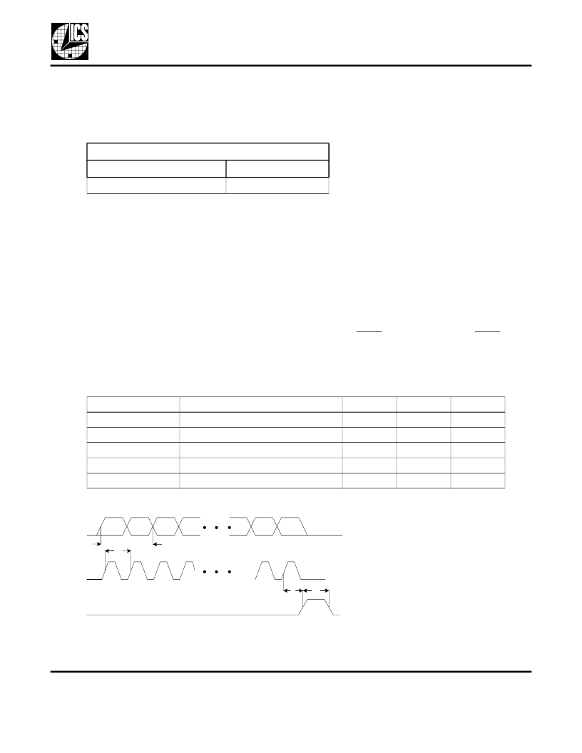
As show in Figure 2, after these 160 bits are clocked into the ICS309, taking STROBE high will send this
data to the internal latch and the CLK output will lock within 10 ms.
Note
: STROBE utilizes a transparent latch that is latched when in the high state. If STROBE is in the high
state and SCLK is pulsed, DATA is clocked directly to the internal latch and the output conditions will
change accordingly. Although this will not damage the ICS309, it is recommended that STROBE be kept
low while DATA is being clocked into the ICS309 in order to avoid unintended changes on the output clocks.
All outputs may be turned off during initialization by bringing the PDTS pin to Ground. When PDTS is
brought high, after the Strobe pin in brought high, the programmed output frequencies will be available.
AC Parameters for Writing to the ICS309
Default Outputs
Output
Frequency
Clocks 1 - 9 (Pins 4, 7-14)
Reference Output
Parameter
Condition
Min.
Max.
Units
t
SETUP
t
HOLD
t
W
t
S
Setup time
10
ns
Hold time after SCLK
10
ns
Data wait time
10
ns
Strobe pulse width
40
ns
SCLK Frequency
30
MHz
DATA
t
hold
t
setup
SCLK
STROBE
t
s
t
w
Figure 2. Timing Diagram for Programming the ICS309
Bit160
Bit2
Bit1
Bit3
Bit159
Bit158
相關(guān)PDF資料 |
PDF描述 |
|---|---|
| ICS309RIT | SERIAL PROGRAMMABLE TRIPLE PLL SS VERSACLOCK SYNTHESIZER |
| ICS341 | Field Programmable SS VersaClock Synthesizer |
| ICS341MIP | Field Programmable SS VersaClock Synthesizer |
| ICS341MLF | Field Programmable SS VersaClock Synthesizer |
| ICS341MP | Field Programmable SS VersaClock Synthesizer |
相關(guān)代理商/技術(shù)參數(shù) |
參數(shù)描述 |
|---|---|
| ICS-310-AGG | 制造商:Samtec Inc 功能描述:CONN DIP SCKT SKT 10 POS 2.54MM SLDR ST TH - Bulk |
| ICS-310-AGT | 制造商:Samtec Inc 功能描述:CONN DIP SCKT SKT 10 POS 2.54MM SLDR ST TH - Bulk |
| ICS-310-ATT | 制造商:Samtec Inc 功能描述:CONN DIP SCKT SKT 10 POS 2.54MM SLDR ST TH - Bulk |
| ICS-310-EGG | 制造商:Samtec Inc 功能描述:CONN DIP SCKT SKT 10 POS 2.54MM SLDR ST TH - Bulk |
| ICS-310-EGT | 制造商:Samtec Inc 功能描述:CONN DIP SCKT SKT 10 POS 2.54MM ST TH - Bulk |
發(fā)布緊急采購,3分鐘左右您將得到回復(fù)。