- 您現(xiàn)在的位置:買賣IC網(wǎng) > PDF目錄385436 > HYS72T256000ER-3.7-B (QIMONDA AG) 240-Pin Registered DDR2 SDRAM Modules PDF資料下載
參數(shù)資料
| 型號(hào): | HYS72T256000ER-3.7-B |
| 廠商: | QIMONDA AG |
| 元件分類: | DRAM |
| 英文描述: | 240-Pin Registered DDR2 SDRAM Modules |
| 中文描述: | 256M X 72 DDR DRAM MODULE, 0.5 ns, DMA240 |
| 封裝: | GREEN, RDIMM-240 |
| 文件頁數(shù): | 18/33頁 |
| 文件大?。?/td> | 892K |
| 代理商: | HYS72T256000ER-3.7-B |
第1頁第2頁第3頁第4頁第5頁第6頁第7頁第8頁第9頁第10頁第11頁第12頁第13頁第14頁第15頁第16頁第17頁當(dāng)前第18頁第19頁第20頁第21頁第22頁第23頁第24頁第25頁第26頁第27頁第28頁第29頁第30頁第31頁第32頁第33頁

Internet Data Sheet
Rev. 1.0, 2006-10
10202006-EHWJ-OT02
18
HYS72T256000ER-[3.7/5]-B
Registerd DDR2 SDRAM Module
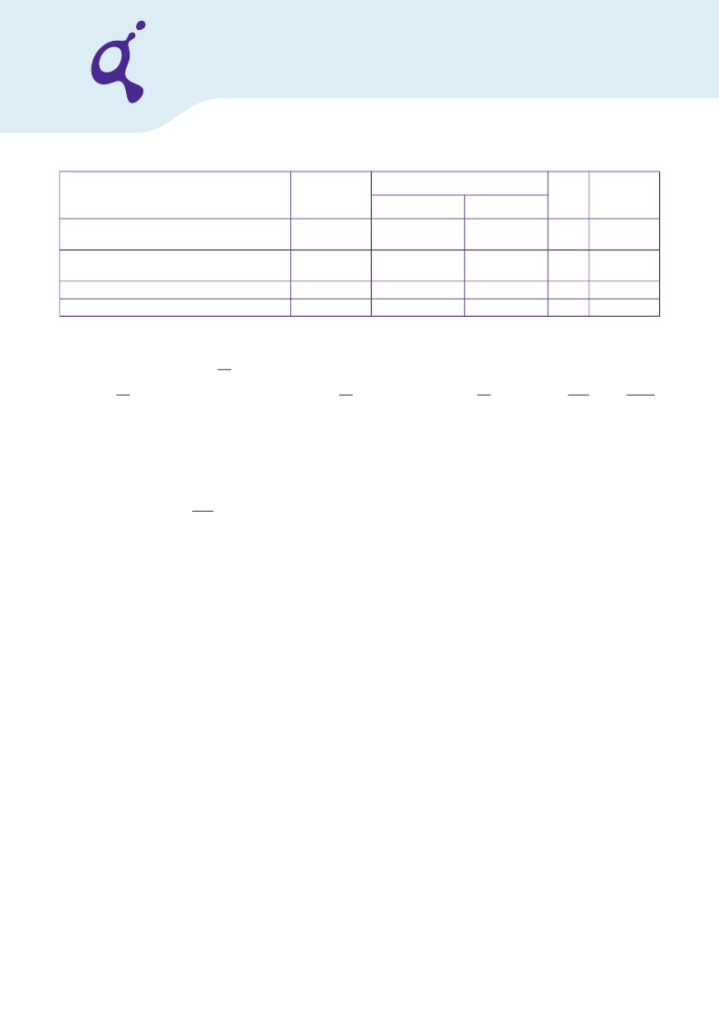
Exit active power-down mode to Read
command (slow exit, lower power)
Exit precharge power-down to any valid
command (other than NOP or Deselect)
Exit Self-Refresh to non-Read command
Exit Self-Refresh to Read command
t
XARDS
6 – AL
—
t
CK
22)
t
XP
2
—
t
CK
t
XSNR
t
XSRD
t
RFC
+10
200
—
—
ns
t
CK
1) For details and notes see the relevant Qimonda component data sheet
2)
V
DDQ
= 1.8 V
±
0.1 V;
V
DD
= 1.8 V
±
0.1 V. See notes
5)6)7)8)
3) Timing that is not specified is illegal and after such an event, in order to guarantee proper operation, the DRAM must be powered down
and then restarted through the specified initialization sequence before normal operation can continue.
4) Timings are guaranteed with CK/CK differential Slew Rate of 2.0 V/ns. For DQS signals timings are guaranteed with a differential Slew
Rate of 2.0 V/ns in differential strobe mode and a Slew Rate of 1 V/ns in single ended mode.
5) The CK / CK input reference level (for timing reference to CK / CK) is the point at which CK and CK cross. The DQS / DQS, RDQS/ RDQS,
input reference level is the crosspoint when in differential strobe mode.
6) Inputs are not recognized as valid until
V
REF
stabilizes. During the period before
V
REF
stabilizes, CKE = 0.2 x
V
DDQ
is recognized as low.
7) The output timing reference voltage level is
V
TT
.
8) For each of the terms, if not already an integer, round to the next highest integer.
t
CK
refers to the application clock period. WR refers to
the WR parameter stored in the MR.
9) The clock frequency is allowed to change during self-refresh mode or precharge power-down mode.
10) For timing definition, refer to the Component data sheet.
11) Consists of data pin skew and output pattern effects, and p-channel to n-channel variation of the output drivers as well as output Slew Rate
mis-match between DQS / DQS and associated DQ in any given cycle.
12) MIN (
t
CL
,
t
CH
) refers to the smaller of the actual clock low time and the actual clock high time as provided to the device (i.e. this value can
be greater than the minimum specification limits for
t
CL
and
t
CH
).
13) The
t
HZ
,
t
RPST
and
t
LZ
,
t
RPRE
parameters are referenced to a specific voltage level, which specify when the device output is no longer driving
(
t
t
), or begins driving (
t
t
).
t
and
t
transitions occur in the same access time windows as valid data transitions.These
parameters are verified by design and characterization, but not subject to production test.
14) The Auto-Refresh command interval has be reduced to 3.9 μs when operating the DDR2 DRAM in a temperature range between 85
°
C
and 95
°
C.
15) 0 °C
≤
T
CASE
≤
85
°
C
16) 85
°
C
<
T
CASE
≤
95
°
C
17) A maximum of eight Auto-Refresh commands can be posted to any given DDR2 SDRAM device.
18) The
t
timing parameter depends on the page size of the DRAM organization. See
Table 2 “Ordering Information for RoHS
Compliant Products” on Page 4
.
19) The maximum limit for the
t
parameter is not a device limit. The device operates with a greater value for this parameter, but system
performance (bus turnaround) degrades accordingly.
20) WR must be programmed to fulfill the minimum requirement for the
t
timing parameter, where
WR
[cycles] =
t
(ns)/
t
(ns) rounded
up to the next integer value.
t
= WR + (
t
/
t
). For each of the terms, if not already an integer, round to the next highest integer.
t
CK
refers to the application clock period. WR refers to the WR parameter stored in the MRS.
21) Minimum
t
WTR
is two clocks when operating the DDR2-SDRAM at frequencies
≤ 200 ΜΗ
z.
22) User can choose two different active power-down modes for additional power saving via MRS address bit A12. In “standard active power-
down mode” (MR, A12 = “0”) a fast power-down exit timing
t
XARD
can be used. In “l(fā)ow active power-down mode” (MR, A12 =”1”) a slow
power-down exit timing
t
XARDS
has to be satisfied.
Parameter
Symbol
DDR2–533
Unit
Note
1)2)3)4)5)
6)7)
Min.
Max.
相關(guān)PDF資料 |
PDF描述 |
|---|---|
| HYS72T256000ER-5-B | 240-Pin Registered DDR2 SDRAM Modules |
| HYS72T256020EU-2.5-B | 240-Pin unbuffered DDR2 SDRAM Modules |
| HYS72T256020EU-25F-B | 240-Pin unbuffered DDR2 SDRAM Modules |
| HYS72T256020EU-3.7-B | 240-Pin unbuffered DDR2 SDRAM Modules |
| HYS72T256020EU-3-B | 240-Pin unbuffered DDR2 SDRAM Modules |
相關(guān)代理商/技術(shù)參數(shù) |
參數(shù)描述 |
|---|---|
| HYS72T256000ER-5-B | 制造商:QIMONDA 制造商全稱:QIMONDA 功能描述:240-Pin Registered DDR2 SDRAM Modules |
| HYS72T256000HR | 制造商:QIMONDA 制造商全稱:QIMONDA 功能描述:240-Pin Registered DDR SDRAM Modules |
| HYS72T256000HR-3.7-A | 制造商:QIMONDA 制造商全稱:QIMONDA 功能描述:240-Pin Registered DDR SDRAM Modules |
| HYS72T256000HR-3S-A | 制造商:QIMONDA 制造商全稱:QIMONDA 功能描述:240-Pin Registered DDR SDRAM Modules |
| HYS72T256000HR-5-A | 制造商:QIMONDA 制造商全稱:QIMONDA 功能描述:240-Pin Registered DDR SDRAM Modules |
發(fā)布緊急采購(gòu),3分鐘左右您將得到回復(fù)。