- 您現(xiàn)在的位置:買賣IC網(wǎng) > PDF目錄385436 > HYS72T1G042ER (QIMONDA) 240-Pin Dual Die Registered DDR2 SDRAM Modules PDF資料下載
參數(shù)資料
| 型號(hào): | HYS72T1G042ER |
| 廠商: | QIMONDA |
| 英文描述: | 240-Pin Dual Die Registered DDR2 SDRAM Modules |
| 中文描述: | 240針雙模具注冊(cè)DDR2 SDRAM內(nèi)存模塊 |
| 文件頁數(shù): | 14/31頁 |
| 文件大小: | 859K |
| 代理商: | HYS72T1G042ER |
第1頁第2頁第3頁第4頁第5頁第6頁第7頁第8頁第9頁第10頁第11頁第12頁第13頁當(dāng)前第14頁第15頁第16頁第17頁第18頁第19頁第20頁第21頁第22頁第23頁第24頁第25頁第26頁第27頁第28頁第29頁第30頁第31頁
Internet Data Sheet
Rev. 1.0, 2007-04
04242007-NQ2Z-YM3O
14
HYS72T1G042ER–5–B
Registerd DDR2 SDRAM Module
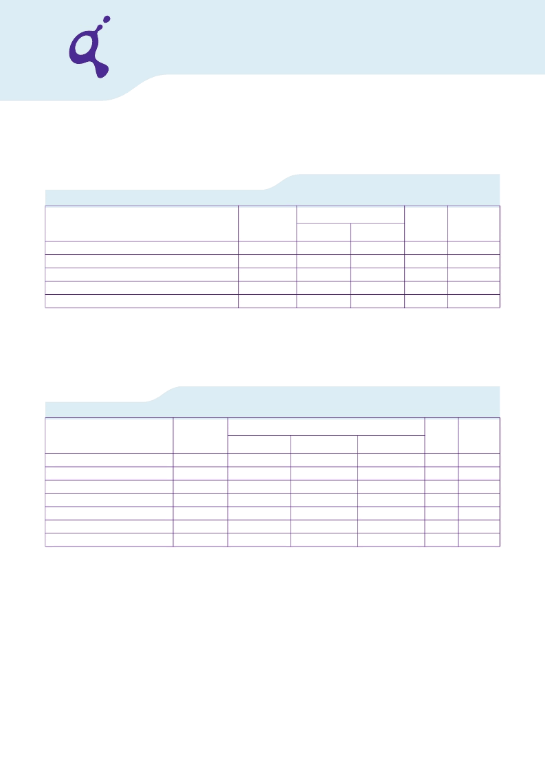
3.2
DC Operating Conditions
This chapter contains the DC operating conditions tables.
TABLE 10
Operating Conditions
TABLE 11
Supply Voltage Levels and DC Operating Conditions
Parameter
Symbol
Values
Unit
Note
Min.
Max.
Operating temperature (ambient)
DRAM Case Temperature
Storage Temperature
Barometric Pressure (operating & storage)
Operating Humidity (relative)
T
OPR
T
CASE
T
STG
P
Bar
H
OPR
0
0
– 50
+69
10
+65
+95
+100
+105
90
°
C
°
C
°
C
kPa
%
1)2)3)4)
1) DRAM Component Case Temperature is the surface temperature in the center on the top side of any of the DRAMs.
2) Within the DRAM Component Case Temperature Range all DRAM specifications will be supported
3) Above 85 °C DRAM Case Temperature the Auto-Refresh command interval has to be reduced to
t
REFI
= 3.9
μ
s
4) When operating this product in the 85 °C to 95 °C
T
CASE
temperature range, the High Temperature Self Refresh has to be enabled by
setting EMR(2) bit A7 to “1”. When the High Temperature Self Refresh is enabled there is an increase of
I
DD6
by approximately 50 %.
5) Up to 3000 m.
5)
Parameter
Symbol
Values
Unit
Note
Min.
Typ.
Max.
Device Supply Voltage
Output Supply Voltage
Input Reference Voltage
SPD Supply Voltage
DC Input Logic High
DC Input Logic Low
In / Output Leakage Current
V
DD
V
DDQ
V
REF
V
DDSPD
V
IH(DC)
V
IL (DC
)
I
L
1.7
1.7
0.49
×
V
DDQ
1.7
V
REF
+ 0.125
– 0.30
– 5
1.8
1.8
0.5
×
V
DDQ
—
—
—
—
1.9
1.9
0.51
×
V
DDQ
3.6
V
DDQ
+ 0.3
V
REF
– 0.125
5
V
V
V
V
V
V
μ
A
1)
1) Under all conditions,
V
DDQ
must be less than or equal to
V
DD
2) Peak to peak AC noise on
V
REF
may not exceed ± 2 %
V
REF
(DC).
V
REF
is also expected to track noise in
V
DDQ
.
3) Input voltage for any connector pin under test of 0 V
≤
V
IN
≤
V
DDQ
+ 0.3 V; all other pins at 0 V. Current is per pin
2)
3)
相關(guān)PDF資料 |
PDF描述 |
|---|---|
| HYS72T1G042ER-5-B | 240-Pin Dual Die Registered DDR2 SDRAM Modules |
| HYS72T1G242EP | 240-Pin Dual Die Registered DDR2 SDRAM Modules |
| HYS72T1G242EP-2.5-C | 240-Pin Dual Die Registered DDR2 SDRAM Modules |
| HYS72T1G242EP-25F-C | 240-Pin Dual Die Registered DDR2 SDRAM Modules |
| HYS72T1G242EP-3.7-C | 240-Pin Dual Die Registered DDR2 SDRAM Modules |
相關(guān)代理商/技術(shù)參數(shù) |
參數(shù)描述 |
|---|---|
| HYS72T1G042ER-5-B | 制造商:QIMONDA 制造商全稱:QIMONDA 功能描述:240-Pin Dual Die Registered DDR2 SDRAM Modules |
| HYS72T1G242EP | 制造商:QIMONDA 制造商全稱:QIMONDA 功能描述:240-Pin Dual Die Registered DDR2 SDRAM Modules |
| HYS72T1G242EP-2.5-C | 制造商:QIMONDA 制造商全稱:QIMONDA 功能描述:240-Pin Dual Die Registered DDR2 SDRAM Modules |
| HYS72T1G242EP-25F-C | 制造商:QIMONDA 制造商全稱:QIMONDA 功能描述:240-Pin Dual Die Registered DDR2 SDRAM Modules |
| HYS72T1G242EP-3.7-C | 制造商:QIMONDA 制造商全稱:QIMONDA 功能描述:240-Pin Dual Die Registered DDR2 SDRAM Modules |
發(fā)布緊急采購,3分鐘左右您將得到回復(fù)。