- 您現(xiàn)在的位置:買賣IC網(wǎng) > PDF目錄385433 > HYMP112S64MP8-C4 (HYNIX SEMICONDUCTOR INC) SCREW LOCKS MALE PDF資料下載
參數(shù)資料
| 型號: | HYMP112S64MP8-C4 |
| 廠商: | HYNIX SEMICONDUCTOR INC |
| 元件分類: | DRAM |
| 英文描述: | SCREW LOCKS MALE |
| 中文描述: | 128M X 64 DDR DRAM MODULE, 0.5 ns, ZMA200 |
| 封裝: | ROHS COMPLIANT, DIMM-200 |
| 文件頁數(shù): | 9/17頁 |
| 文件大小: | 405K |
| 代理商: | HYMP112S64MP8-C4 |

HYMP112S64(L)MP8
Rev. 0.1/ July 2004
9
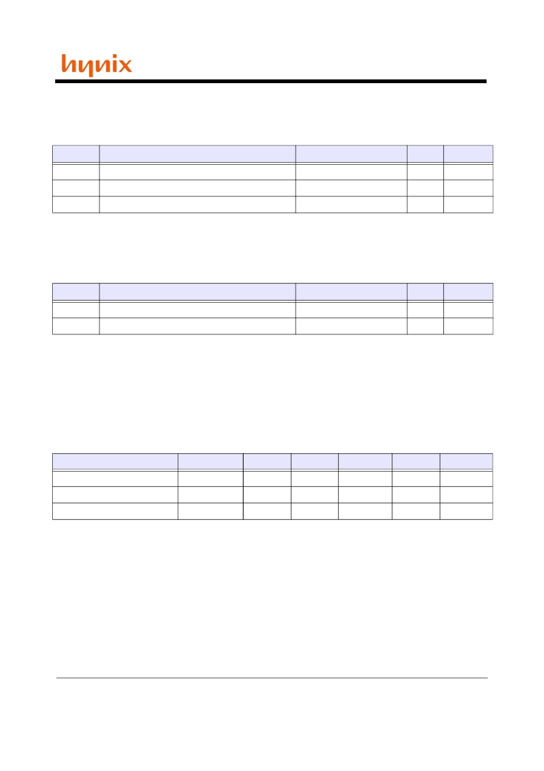
Output Buffer Levels
Output AC Test Conditions
Output DC Current Drive
OCD defalut characteristics
Note:
1. Absolute Specifications
(0°C
≤
T
CASE
≤
+95°C; VDD = +1.8V ±0.1V, VDDQ = +1.8V ±0.1V)
2. Impedance measurement condition for output source dc current: VDDQ = 1.7V; VOUT = 1420mV; (VOUT-VDDQ)/Ioh must be less
than 23.4 ohms for values of VOUT between VDDQ and VDDQ-280mV. Impedance measurement condition for output sink dc current:
VDDQ = 1.7V; VOUT = 280mV; VOUT/Iol must be less than 23.4 ohms for values of VOUT between 0V and 280mV.
3. Mismatch is absolute value between pull-up and pull-dn, both are measured at same temperature and voltage.
4. Slew rate measured from vil(ac) to vih(ac).
5. The absolute value of the slew rate as measured from DC to DC is equal to or greater than the slew rate as measured from AC to AC.
6. DRAM output slew rate specification applies to 400MT/s & 533MT/s speed bins. Output slew rate at 667&800MT/s will be added with
JEDEC process.
Symbol
Parameter
SSTL_18 Class II
Units
Notes
V
OH
Minimum Required Output Pull-up under AC Test Load
V
TT
+ 0.603
V
V
OL
Maximum Required Output Pull-down under AC Test Load
V
TT
- 0.603
V
V
OTR
Output Timing Measurement Reference Level
0.5 * V
DDQ
V
1
1. The VDDQ of the device under test is referenced.
Symbol
Parameter
SSTl_18 Class II
Units
Notes
I
OH(dc)
Output Minimum Source DC Current
- 13.4
mA
1, 3, 4
I
OL(dc)
Output Minimum Sink DC Current
13.4
mA
2, 3, 4
1. V
DDQ
= 1.7 V; V
OUT
= 1420 mV. (V
OUT
- V
DDQ
)/I
OH
must be less than 21 ohm for values of V
OUT
between V
DDQ
and V
DDQ
- 280 mV.
2. V
DDQ
= 1.7 V; V
OUT
= 280 mV. V
OUT
/I
OL
must be less than 21 ohm for values of V
OUT
between 0 V and 280 mV.
3. The dc value of V
REF
applied to the receiving device is set to V
TT
4. The values of I
OH(dc)
and I
OL(dc)
are based on the conditions given in Notes 1 and 2. They are used to test device drive current
capability to ensure V
IH
min plus a noise margin and V
IL
max minus a noise margin are delivered to an SSTL_18 receiver. The actual
current values are derived by shifting the desired driver operating point (see Section 3.3) along a 21 ohm load line to define a
convenient driver current for measurement.
Description
Parameter
Min
Nom
Max
Unit
Notes
Output impedance
12.6
18
23.4
ohms
1,2
Pull-up and pull-down mismatch
0
4
ohms
1,2,3
Output slew rate
Sout
1.5
-
5
V/ns
1,4,5,6
相關(guān)PDF資料 |
PDF描述 |
|---|---|
| HYMP112S64MP8-C5 | SCREW LOCKS MALE |
| HYMP112S64MP8-E3 | SCREW LOCKS MALE |
| HYMP112S64MP8-E4 | SCREW LOCKS FEMALE SETS |
| HYS72D64300HBR-5-C | 184-Pin Registered Double Data Rate SDRAM Module |
| HYS72D64300HBR-6-C | 184-Pin Registered Double Data Rate SDRAM Module |
相關(guān)代理商/技術(shù)參數(shù) |
參數(shù)描述 |
|---|---|
| HYMP112S64MP8-C5 | 制造商:HYNIX 制造商全稱:Hynix Semiconductor 功能描述:DDR2 SDRAM SO-DIMM |
| HYMP112S64MP8-E3 | 制造商:HYNIX 制造商全稱:Hynix Semiconductor 功能描述:200pin Unbuffered DDR2 SDRAM SO-DIMMs based on 512 Mb 1st ver. |
| HYMP112S64MP8-E4 | 制造商:HYNIX 制造商全稱:Hynix Semiconductor 功能描述:DDR2 SDRAM SO-DIMM |
| HYMP112U64CP8-C4 | 制造商:HYNIX 制造商全稱:Hynix Semiconductor 功能描述:240pin DDR2 SDRAM Unbuffered DIMMs |
| HYMP112U64CP8-S5 | 制造商:HYNIX 制造商全稱:Hynix Semiconductor 功能描述:240pin DDR2 SDRAM Unbuffered DIMMs |
發(fā)布緊急采購,3分鐘左右您將得到回復(fù)。