- 您現(xiàn)在的位置:買賣IC網(wǎng) > PDF目錄370789 > HYB3164405T-50 (SIEMENS A G) 16M x 4-Bit Dynamic RAM PDF資料下載
參數(shù)資料
| 型號: | HYB3164405T-50 |
| 廠商: | SIEMENS A G |
| 元件分類: | DRAM |
| 英文描述: | 16M x 4-Bit Dynamic RAM |
| 中文描述: | 16M X 4 EDO DRAM, 50 ns, PDSO34 |
| 文件頁數(shù): | 10/32頁 |
| 文件大小: | 473K |
| 代理商: | HYB3164405T-50 |
第1頁第2頁第3頁第4頁第5頁第6頁第7頁第8頁第9頁當前第10頁第11頁第12頁第13頁第14頁第15頁第16頁第17頁第18頁第19頁第20頁第21頁第22頁第23頁第24頁第25頁第26頁第27頁第28頁第29頁第30頁第31頁第32頁
Semiconductor Group
98
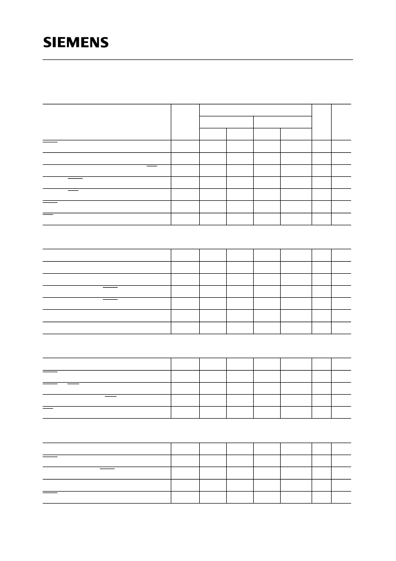
HYB3164(5)405J/T(L)-50/-60
16M x 4-DRAM
CAS to output in low-Z
t
CLZ
t
OFF
t
OEZ
t
DZC
t
DZO
t
CDD
t
ODD
0
–
0
–
ns
8
Output buffer turn-off delay
0
13
0
15
ns
12
Output buffer turn-off delay from OE
0
13
0
15
ns
12
Data to CAS low delay
0
–
0
–
ns
13
Data to OE low delay
0
–
0
–
ns
13
CAS high to data delay
13
–
15
–
ns
14
OE high to data delay
13
–
15
–
ns
14
Write Cycle
Write command hold time
t
WCH
t
WP
t
WCS
t
RWL
t
CWL
t
DS
t
DH
8
–
10
–
ns
Write command pulse width
7
–
10
–
ns
Write command setup time
0
–
0
–
ns
15
Write command to RAS lead time
8
–
10
–
ns
Write command to CAS lead time
8
–
10
–
ns
Data setup time
0
–
0
–
ns
16
Data hold time
7
–
10
–
ns
16
Read-modify-Write Cycle
Read-write cycle time
t
RWC
t
RWD
t
CWD
t
AWD
t
OEH
111
–
135
–
ns
RAS to WE delay time
67
–
79
–
ns
15
CAS to WE delay time
30
–
34
–
ns
15
Column address to WE delay time
42
–
49
–
ns
15
OE command hold time
7
–
10
–
ns
Hyper Page Mode (EDO) Cycle
Hyper page mode (EDO) cycle time
t
HPC
t
CP
t
CPA
t
COH
t
RAS
20
–
25
–
ns
CAS precharge time
8
–
10
–
ns
Access time from CAS precharge
–
27
–
35
ns
7
Output data hold time
5
–
5
–
ns
RAS pulse width in hyper page mode
50
200k
60
200k
ns
AC Characteristics
(cont’d)
5)6)
T
A
= 0 to 70 C,
V
CC
= 3.3 V
±
0.3V ,
t
T
= 2 ns
Parameter
Symbol
Limit Values
Unit
Note
-50
-60
min.
max.
min.
max.
發(fā)布緊急采購,3分鐘左右您將得到回復。