- 您現(xiàn)在的位置:買賣IC網(wǎng) > PDF目錄370787 > HYB316400BTL-50 (SIEMENS AG) 3.3V 4M x 4-Bit Dynamic RAM PDF資料下載
參數(shù)資料
| 型號: | HYB316400BTL-50 |
| 廠商: | SIEMENS AG |
| 英文描述: | 3.3V 4M x 4-Bit Dynamic RAM |
| 中文描述: | 3.3 4米× 4位動態(tài)隨機存儲器 |
| 文件頁數(shù): | 6/26頁 |
| 文件大?。?/td> | 253K |
| 代理商: | HYB316400BTL-50 |
Semiconductor Group
6
HYB 3116(7)400BJ/BT(L) -50/-60/-70
3.3V 4Mx4-DRAM
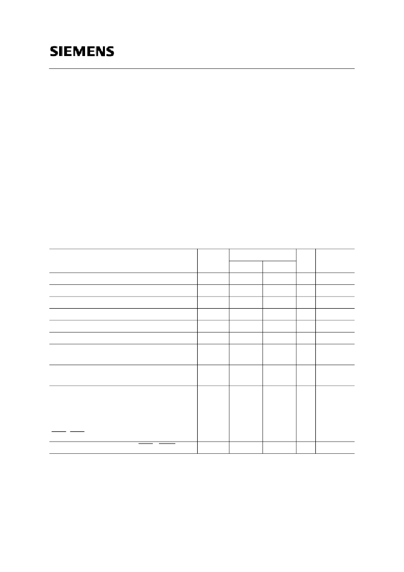
Absolute Maximum Ratings
Operating temperature range ............................................................................................0 to 70 °C
Storage temperature range.........................................................................................– 55 to 150 °C
Input/output voltage ................................................................................-0.5 to min(Vcc+0.5, 4.6) V
Power supply voltage.................................................................................................- 0.5 V to 4.6 V
Power dissipation.................................................................................................................... 0.5 W
Data out current (short circuit) ................................................................................................ 50 mA
Note:
Stresses above those listed under “Absolute Maximum Ratings” may cause permanent damage of
the device. Exposure to absolute maximum rating conditions for extended periods may affect device
reliability.
DC Characteristics
(values in brackets for HYB3117400)
T
A
= 0 to 70 °C,
V
SS
= 0 V,
V
CC
= 3.3 V
±
0.3 V,
t
T
= 5 ns
Parameter
Symbol
Limit Values
Unit Test
Condition
min.
max.
Input high voltage
V
IH
V
IL
V
OH
V
OL
V
OH
V
OL
I
I(L)
2.0
Vcc+0.5
V
1)
Input low voltage
TTL Output high voltage (
I
OUT
= – 2 mA)
TTL Output low voltage (
I
OUT
= 2 mA)
CMOS Output high voltage (
I
OUT
= –100 uA)
CMOS Output low voltage (
I
OUT
= 100 uA)
Input leakage current
(0 V
≤
V
IH
≤
Vcc + 0.3V, all other pins = 0 V)
Output leakage current
(DO is disabled, 0 V
≤
V
OUT
≤
Vcc + 0.3V)
Average
V
CC
supply current:
– 0.5
0.8
V
1)
2.4
–
V
1)
–
0.4
V
1)
VCC-0.2
–
V
–
0.2
V
μ
A
– 10
10
1)
I
O(L)
– 10
10
μ
A
1)
-50 ns version
-60 ns version
-70 ns version
(RAS, CAS, address cycling,
t
RC
=
t
RC
min.)
Standby
V
CC
supply current (RAS = CAS =
V
IH
)
I
CC2
I
CC1
–
–
–
100(120)
90 (110)
80 (100)
mA
mA
mA
2) 3) 4)
2) 3) 4)
2) 3) 4)
–
2
mA
–
相關PDF資料 |
PDF描述 |
|---|---|
| HYB3117400BJ-50 | 3.3V 4M x 4-Bit Dynamic RAM |
| HYB3116400BJ-50 | 3.3V 4M x 4-Bit Dynamic RAM |
| HYB3117400BT-70 | 3.3V 4M x 4-Bit Dynamic RAM |
| HYB3116400BT-70 | 3.3V 4M x 4-Bit Dynamic RAM |
| HYB3117400BT-60 | 3.3V 4M x 4-Bit Dynamic RAM |
相關代理商/技術參數(shù) |
參數(shù)描述 |
|---|---|
| HYB3164160AT | 制造商:INFINEON 制造商全稱:Infineon Technologies AG 功能描述:4M x 16-Bit Dynamic RAM |
| HYB3164160AT-40 | 制造商:INFINEON 制造商全稱:Infineon Technologies AG 功能描述:4M x 16-Bit Dynamic RAM |
| HYB3164160AT-50 | 制造商:INFINEON 制造商全稱:Infineon Technologies AG 功能描述:4M x 16-Bit Dynamic RAM |
| HYB3164160AT-60 | 制造商:INFINEON 制造商全稱:Infineon Technologies AG 功能描述:4M x 16-Bit Dynamic RAM |
| HYB3164160ATL-50 | 制造商:INFINEON 制造商全稱:Infineon Technologies AG 功能描述:4M x 16-Bit Dynamic RAM |
發(fā)布緊急采購,3分鐘左右您將得到回復。