- 您現(xiàn)在的位置:買賣IC網(wǎng) > PDF目錄385428 > HY5DU56822ELFP-K (Hynix Semiconductor Inc.) 256Mb DDR SDRAM PDF資料下載
參數(shù)資料
| 型號: | HY5DU56822ELFP-K |
| 廠商: | Hynix Semiconductor Inc. |
| 英文描述: | 256Mb DDR SDRAM |
| 中文描述: | 256Mb的DDR SDRAM內(nèi)存 |
| 文件頁數(shù): | 24/29頁 |
| 文件大小: | 260K |
| 代理商: | HY5DU56822ELFP-K |
第1頁第2頁第3頁第4頁第5頁第6頁第7頁第8頁第9頁第10頁第11頁第12頁第13頁第14頁第15頁第16頁第17頁第18頁第19頁第20頁第21頁第22頁第23頁當(dāng)前第24頁第25頁第26頁第27頁第28頁第29頁

Rev. 1.1 / J une 2006
24
1
HY5DU56822E(L)FP
HY5DU561622E(L)FP
Note:
1. All voltages referenced to Vss.
2. Tests for ac timing, IDD, and electrical, ac and dc characteristics, may be conducted at nominal reference/supply voltage levels,
but the related specifications and device operation are guaranteed for the full voltage range specified.
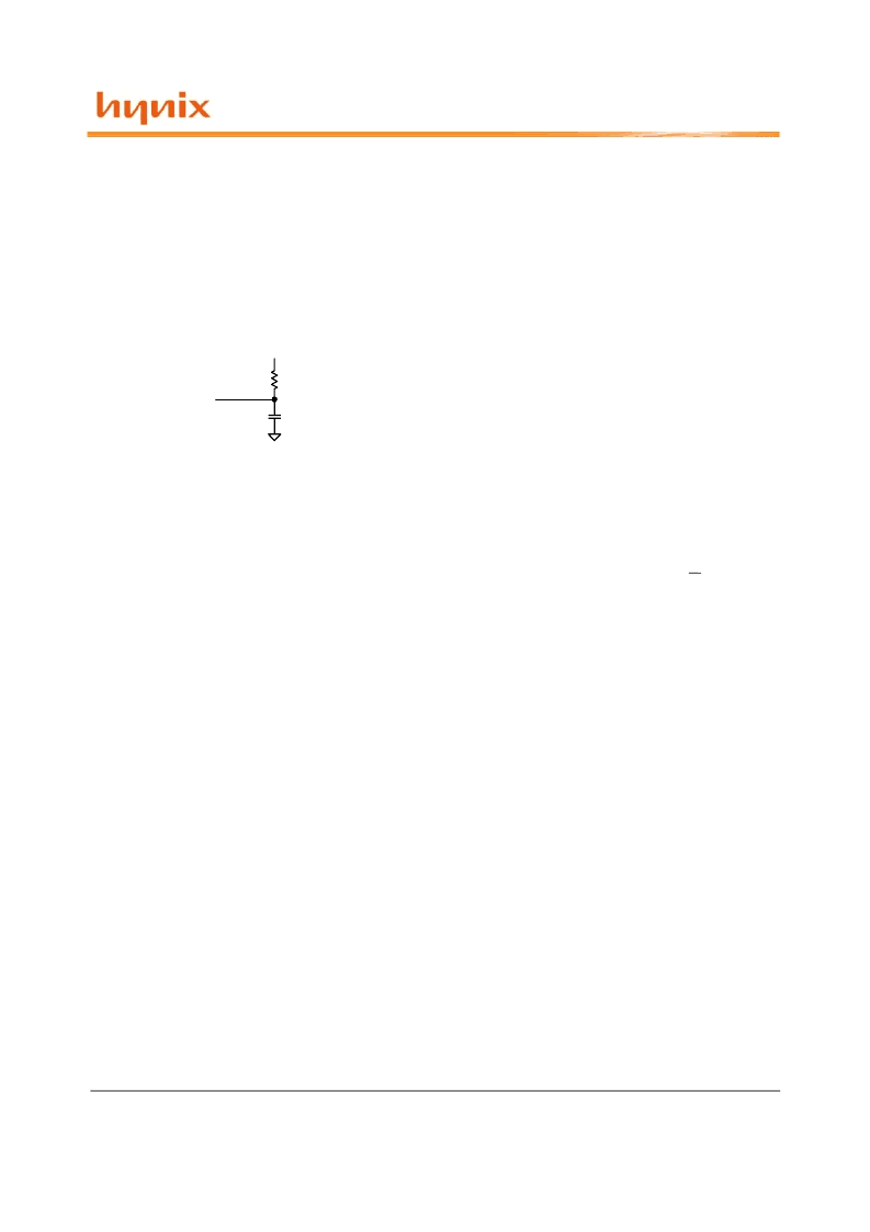
3. Below figure represents the timing reference load used in defining the relevant timing parameters of the part. It is not intended to
be either a precise representation of the typical system environment nor a depiction of the actual load presented by a production
tester. System designers will use IBIS or other simulation tools to correlate the timing reference load to a system environment.
Manufacturers will correlate to their production test conditions (generally a coaxial transmission line terminated at the tester elec-
tronics).
4. AC timing and IDD tests may use a VIL to VIH swing of up to 1.5 V in the test environment, but input timing is still referenced to
VREF (or to the crossing point for CK, /CK), and parameter specifications are guaranteed for the specified ac input levels under
normal use conditions. The minimum slew rate for the input signals is 1 V/ns in the range between VIL(ac) and VIH(ac).
5. The ac and dc input level specifications are as defined in the SSTL_2 Standard (i.e., the receiver will effectively switch as a result
of the signal crossing the ac input level and will remain in that state as long as the signal does not ring back above (below) the
dc input LOW (HIGH) level.
6. Inputs are not recognized as valid until VREF stabilizes.
Exception: during the period before VREF stabilizes, CKE <
0.2VDDQ is
recognized as LOW.
7. The CK, /CK input reference level (for timing referenced to CK, /CK) is the point at which CK and /CK cross; the input reference
level for signals other than CK, /CK is VREF.
8. The output timing reference voltage level is VTT.
9
.
Operation or timing that is not specified is illegal
and after such an event, in order to guarantee
proper operation, the DRAM must
be powered
down and then restarted through the specified initialization
sequence before normal operation
can continue.
10. tHZ and tLZ transitions occur in the same access time windows as valid data transitions. These parameters are not referenced to
a specific voltage level but specify when the device output is no longer driving (HZ), or begins driving (LZ).
11. The maximum limit for this parameter is not a device limit. The device will operate with a greater value for this parameter but
system performance (bus turnaround) will degrade accordingly.
12. The specific requirement is that DQS be valid (HIGH, LOW, or at some point on a valid transition) on or before this CK edge. A
valid transition is defined as monotonic and meeting the input slew rate specifications of the device. When no writes were previ-
ously in progress on the bus, DQS will be transitioning from High-Z to logic LOW. If a previous write was in progress, DQS could
be HIGH, LOW, or transitioning from HIGH to LOW at this time, depending on tDQSS.
13. A maximum of eight AUTO REFRESH commands can be posted to any given DDR SDRAM device.
14. For command/address input slew rate
≥
1.0 V/ns.
15. For command/address input slew rate
≥
0.5 V/ns and
<
1.0 V/ns
16. For CK &
/
CK slew rate
≥
1.0 V/ns (single-ended)
17. These parameters guarantee device timing, but they are not necessarily tested on each device.
They may be guaranteed by device design or tester correlation.
18. Slew Rate is measured between VOH(ac) and VOL(ac).
19. Min (tCL, tCH) refers to the smaller of the actual clock low time and the actual clock high time as provided to the device (i.e. this
value can be greater than the minimum specification limits for tCL and tCH).
For example, tCL and tCH are = 50% of the period, less the half period jitter (tJIT(HP)) of the clock source, and less the half
period jitter due to crosstalk (tJIT(crosstalk)) into the clock traces.
Figure: Timing Reference Load
VDDQ
50
Output
(VOUT)
30 pF
Ω
相關(guān)PDF資料 |
PDF描述 |
|---|---|
| HY5DU56822ELFP-L | 256Mb DDR SDRAM |
| HY5DV281622DT | 128M(8Mx16) GDDR SDRAM |
| HY5DV281622DT-33 | 128M(8Mx16) GDDR SDRAM |
| HY5DV281622DT-36 | 128M(8Mx16) GDDR SDRAM |
| HY5DV281622DT-4 | 128M(8Mx16) GDDR SDRAM |
相關(guān)代理商/技術(shù)參數(shù) |
參數(shù)描述 |
|---|---|
| HY5DU56822ELFP-L | 制造商:HYNIX 制造商全稱:Hynix Semiconductor 功能描述:256Mb DDR SDRAM |
| HY5DU56822FLTP-D43 | 制造商:HYNIX 制造商全稱:Hynix Semiconductor 功能描述:256Mb DDR SDRAM |
| HY5DU56822FLTP-D43I | 制造商:HYNIX 制造商全稱:Hynix Semiconductor 功能描述:256Mb DDR SDRAM |
| HY5DU56822FLTP-D5 | 制造商:HYNIX 制造商全稱:Hynix Semiconductor 功能描述:256Mb DDR SDRAM |
| HY5DU56822FLTP-D5I | 制造商:HYNIX 制造商全稱:Hynix Semiconductor 功能描述:256Mb DDR SDRAM |
發(fā)布緊急采購,3分鐘左右您將得到回復(fù)。