- 您現(xiàn)在的位置:買賣IC網(wǎng) > PDF目錄385415 > HY29F400TT-55 (HYNIX SEMICONDUCTOR INC) x8/x16 Flash EEPROM PDF資料下載
參數(shù)資料
| 型號: | HY29F400TT-55 |
| 廠商: | HYNIX SEMICONDUCTOR INC |
| 元件分類: | DRAM |
| 英文描述: | x8/x16 Flash EEPROM |
| 中文描述: | 256K X 16 FLASH 5V PROM, 55 ns, PDSO48 |
| 封裝: | TSOP-48 |
| 文件頁數(shù): | 8/40頁 |
| 文件大小: | 509K |
| 代理商: | HY29F400TT-55 |
第1頁第2頁第3頁第4頁第5頁第6頁第7頁當(dāng)前第8頁第9頁第10頁第11頁第12頁第13頁第14頁第15頁第16頁第17頁第18頁第19頁第20頁第21頁第22頁第23頁第24頁第25頁第26頁第27頁第28頁第29頁第30頁第31頁第32頁第33頁第34頁第35頁第36頁第37頁第38頁第39頁第40頁
8
Rev. 5.2/May 01
HY29F400
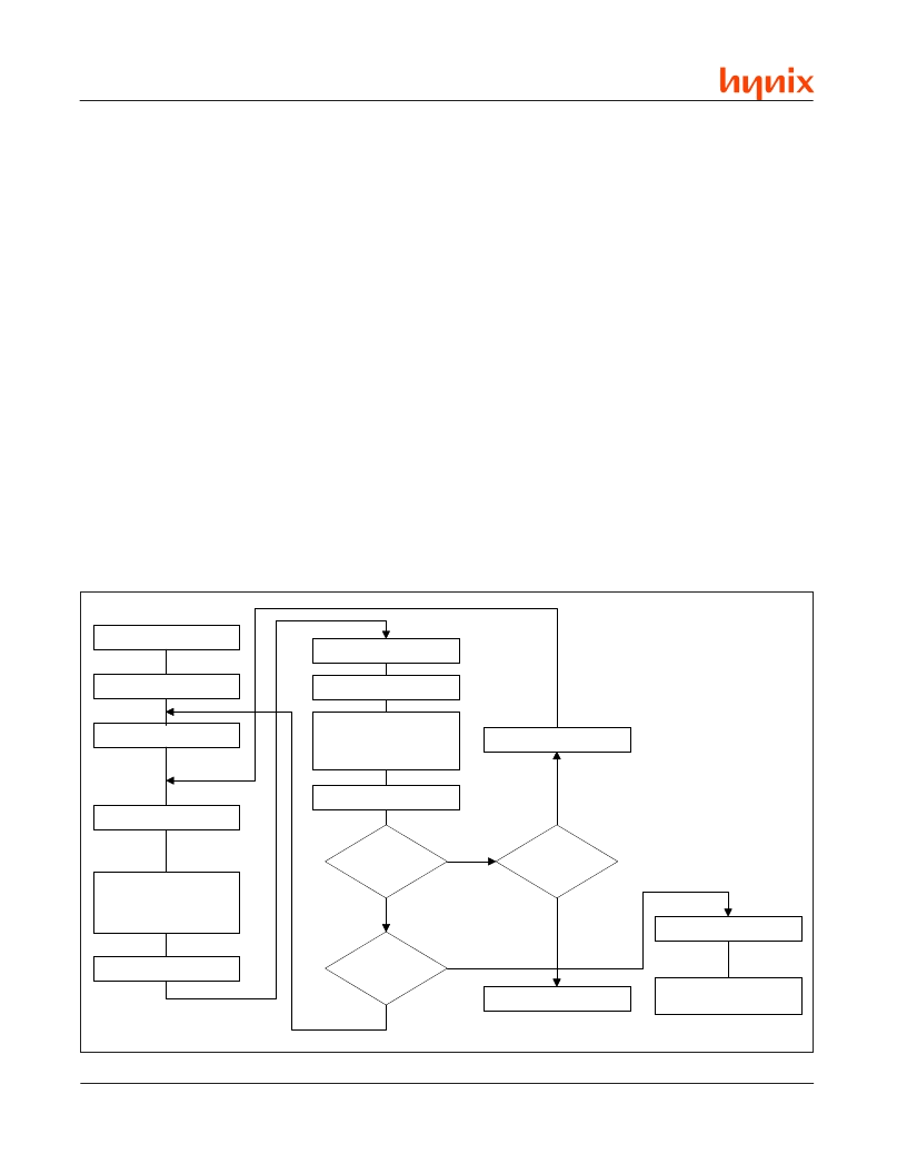
Figure 1. Sector Protect Procedure
If RESET# is asserted during a program or erase
operation, the RY/BY# pin remains Low (busy) until
the internal reset operation is complete, which re-
quires a time of t
READY
(during Automatic Algo-
rithms). The system can thus monitor RY/BY# to
determine when the reset operation completes,
and can perform a read or write operation t
RB
after
RY/BY# goes High. If RESET# is asserted when
a program or erase operation is not executing (RY/
BY# pin is High), the reset operation is completed
within a time of t
RP
. In this case, the host can per-
form a read or write operation t
RH
after the RE-
SET# pin returns High .
The RESET# pin may be tied to the system reset
signal. Thus, a system reset would also reset the
device, enabling the system to read the boot-up
firmware from the Flash memory.
Sector Protect/Unprotect Operations
Hardware sector protection can be invoked to dis-
able program and erase operations in any single
sector or combination of sectors. This function is
typically used to protect data in the device from
unauthorized or accidental attempts to program
or erase the device while it is in the system (e.g.,
by a virus) and is implemented using program-
ming equipment. Sector unprotection re-enables
the program and erase operations in previously
protected sectors.
Table 1 identifies the eleven sectors and the ad-
dress range that each covers for both versions of
the device. The device is shipped with all sectors
unprotected.
The sector protect/unprotect operations require a
high voltage (V
ID
) on address pin A[9] and the CE#
and/or OE# control pins, as detailed in Table 3.
When implementing these operations, note that
V
CC
must be applied to the device before applying
V
ID
, and that V
ID
should be removed before remov-
ing V
CC
from the device.
The flow chart in Figure 1 illustrates the proce-
dure for protecting sectors, and timing specifica-
tions and waveforms are shown in the specifica-
tions section of this document. Verification of pro-
tection is accomplished as described in the Elec-
tronic ID Mode section and shown in the flow chart.
START
Set TRYCNT = 1
Set A[9] = OE# = V
ID
Set Address:
A[17:12] = Sector to Protect
CE# = V
IL
RESET# = V
IH
WE# = V
IL
Wait t
WPP1
A[9] = V
A[17:12] = Sector to Protect
OE# = CE# = V
A[6] = A[0] = V
IL
, A[1] = V
IH
Read Data
Data = 0x01
Protect Another
Sector
YES
TRYCNT = 25
NO
Increment TRYCNT
NO
YES
DEVICE FAILURE
YES
NO
Remove V
ID
from A[9]
SECTOR PROTECT
COMPLETE
APPLY V
CC
WE# = V
IH
相關(guān)PDF資料 |
PDF描述 |
|---|---|
| HY29F400TT-70 | x8/x16 Flash EEPROM |
| HY29F400TT-90 | x8/x16 Flash EEPROM |
| HY29F800TG-12 | x8/x16 Flash EEPROM |
| HY29F800 | 8 Megabit (1Mx8/512Kx16), 5 Volt-only, Flash Memory |
| HY29F800BG-70 | x8/x16 Flash EEPROM |
相關(guān)代理商/技術(shù)參數(shù) |
參數(shù)描述 |
|---|---|
| HY29F400TT70 | 制造商:HYNIX 制造商全稱:Hynix Semiconductor 功能描述:4 Megabit (512Kx8/256Kx16) 5 Volt-only Flash Memory |
| HY29F400TT-70 | 制造商:HYNIX 制造商全稱:Hynix Semiconductor 功能描述:x8/x16 Flash EEPROM |
| HY29F400TT90 | 制造商:HYNIX 制造商全稱:Hynix Semiconductor 功能描述:4 Megabit (512Kx8/256Kx16) 5 Volt-only Flash Memory |
| HY29F400TT-90 | 制造商:HYNIX 制造商全稱:Hynix Semiconductor 功能描述:x8/x16 Flash EEPROM |
| HY29F800 | 制造商:HYNIX 制造商全稱:Hynix Semiconductor 功能描述:8 Megabit (1Mx8/512Kx16), 5 Volt-only, Flash Memory |
發(fā)布緊急采購,3分鐘左右您將得到回復(fù)。