- 您現(xiàn)在的位置:買賣IC網(wǎng) > PDF目錄385406 > HT9170 (Holtek Semiconductor Inc.) DTMF Receiver PDF資料下載
參數(shù)資料
| 型號: | HT9170 |
| 廠商: | Holtek Semiconductor Inc. |
| 英文描述: | DTMF Receiver |
| 中文描述: | 雙音多頻接收器 |
| 文件頁數(shù): | 7/12頁 |
| 文件大小: | 124K |
| 代理商: | HT9170 |

HT9170
7
December 20, 1999
Functional Description
Overview
The HT9170 series tone decoders consist of
three band pass filters and two digital decode
circuits to convert a tone (DTMF) signal into
digital code output.
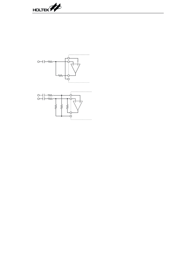
An operational amplifier is built-in to adjust
the input signal (refer to Figure 2).
The pre-filter is a band rejection filter which re-
duces the dialing tone from 350Hz to 400Hz.
The low group filter filters low group frequency
signal output whereas the high group filter fil-
ters high group frequency signal output.
Each filter output is followed by a zero-crossing
detector with hysteresis. When each signal am-
plitude at the output exceeds the specified
level,itistransferredtofullswinglogicsignal.
When input signals are recognized to be effec-
tive, DV becomes high, and the correct tone
code (DTMF) digit is transferred.
Steering control circuit
The steering control circuit is used for measur-
ingtheeffectivesignaldurationandforprotect-
ing against drop out of valid signals. It employs
the analog delay by external RC time-constant
controlled by EST.
The timing is shown in Figure 3. The EST pin is
normally low and draws the RT/GT pin to keep
low through discharge of external RC. When a
valid tone input is detected, EST goes high to
charge RT/GT through RC.
When the voltage of RT/GT changes from 0 to
V
TRT
(2.35V for 5V supply), the input signal is
effective, and the correct code will be created by
the code detector. After D0~D3 are completely
latched, DV output becomes high. When the
voltage of RT/GT falls down from VDD to V
TRT
(i.e.., when there is no input tone), DV output
becomes low, and D0~D3 keeps data until a
next valid tone input is produced.
ByselectingadequateexternalRCvalue,themin-
imum acceptable input tone duration (t
ACC
) and
the minimum acceptable inter-tone rejection (t
IR
)
can be set. External components (R, C) are chosen
by the formula (refer to Figure 5.):
t
ACC
=t
DP
+t
GTP
;
t
IR
=t
DA
+t
GTA
;
where t
ACC
: Tone duration acceptable time
t
DP
: EST output delay time ( L
t
GTP
: Tone present time
t
IR
: Inter-digit pause rejection time
H )
t
DA
: EST output delay time ( H
t
GTA
: Tone absent time
L )
'
%
. - "
.
. "
: ;% * *
'
%
. - "
.
.
: = ; )
!
. 6
.
.
Figure 2. Input operation for amplifier applica-
tion circuits
相關(guān)PDF資料 |
PDF描述 |
|---|---|
| HT9170B | DTMF Receiver |
| HT9170D | DTMF Receiver |
| HT9172 | DTMF Receiver |
| HT9200 | DTMF Generators |
| HT9200A | DTMF Generators |
相關(guān)代理商/技術(shù)參數(shù) |
參數(shù)描述 |
|---|---|
| HT9170A | 制造商:未知廠家 制造商全稱:未知廠家 功能描述:DTMF Receiver |
| HT9170B | 制造商:HOLTEK 制造商全稱:Holtek Semiconductor Inc 功能描述:DTMF Receiver |
| HT9170B(18DIP) | 制造商:未知廠家 制造商全稱:未知廠家 功能描述:Telecomm/Datacomm |
| HT9170B_02 | 制造商:HOLTEK 制造商全稱:Holtek Semiconductor Inc 功能描述:DTMF Receiver |
| HT9170C | 制造商:未知廠家 制造商全稱:未知廠家 功能描述:DTMF Receiver |
發(fā)布緊急采購,3分鐘左右您將得到回復(fù)。